
Refine by:
✖ Clear
Solutions
Services
Format

Accelerated Evolution in Medical Device Miniaturization
Medical device miniaturization is reshaping healthcare with smaller, smarter electronics and real-time sensing. Explore the challenges and manufacturing solutions behind ultra-small medical electronics and implantable devices. Explore medical miniaturization trends.
Subtractive vs. mSAP: Choosing the Right PCB Fabrication Path
Subtractive vs. mSAP for PCBs. Compare processes, features, and when to use each for next-gen electronics. Integrated PCB + iNPACK solutions.
Transitioning from HTE to RTF Copper Foil in PCB Manufacturing
High-Temperature Electrolytic (HTE) copper foil or transition to Reverse Treated Foil (RTF) in both core and outer layers? Learn more.
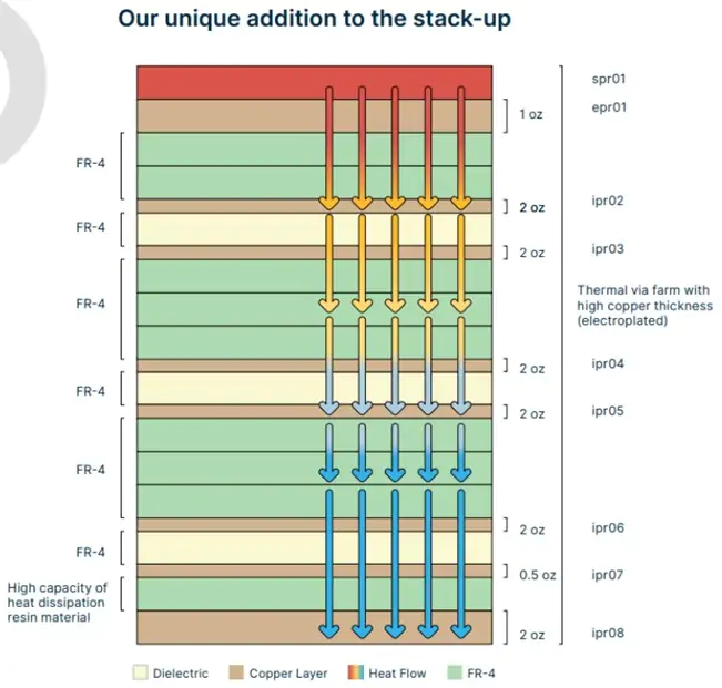
PCB Heat Dissipation Solutions for High-Performance Systems
As the demand for compact, high-performance electronic systems continues to rise, thermal management has become one of the most technically challenging aspects of printed circuit board (PCB) design.

PCB Manufacturing: Processes, Technologies, Standards
A Printed Circuit Board (PCB) is a laminated structure that consists of conductive and insulating layers that serve as the foundation for electronic circuits.
Design Considerations for IC Substrates and Chiplet Integration
This paper explores the key considerations & parameters for IC substrate design, high-speed interconnects, and chiplet integration.

Flex-Rigid PCBs: Why You Should Use Them
Flex Rigid or Rigid Flex PCBs have become a popular choice used in designing today’s electronics by offering greater design flexibility, reduced product weight, sub-compact packaging and simplified PCB assembly.

Panel-Level Packaging vs. Wafer-Level Packaging
In the fast-paced world of electronics, miniaturization, cost-efficiency, and performance optimization are critical. Advanced packaging technologies—Panel-Level Packaging (PLP) and Wafer-Level Packaging (WLP)—are driving this evolution.

Range of IC Packaging Design Formats
A list with descriptions, key features, applications & new developments pertaining to a wide range of IC Packaging Design Formats.


Advanced QFN Technologies - Panel-Level Assembly, Near-Hermetic Sealing & Testing
Advanced QFN Technologies - Panel-Level Assembly, Near-Hermetic Sealing & Testing

Organic QFN IC Packages: Comparing Packaging Options QFN, LGA & Materials
Organic QFN IC package types can be distinguished by variations in mounting style, pin layout, shape and pin count.

QFN IC Packages | Organic Panel Level Process
QFN IC Packages: The QFN (Quad Flat No-lead) package is a versatile and efficient packaging technology widely used in various industries.

PCB Fabrication: Subtractive vs. mSAP
In PCB fabrication, What's the best option? Subtractive or Modified Semi-Additive Process (mSAP)

Faster, More Accurate Production of HDI PCBs
The Future is Clear: See examples of clean, sharp ablation drilling, enabling robust and uniform Via plating for enhanced electrical conductivity in HDI PCBs.

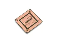
PCBs – The Critical Core Component in Medical Devices & Equipment
Within the realm of PCBs used in the design of medical devices, there exist numerous significant challenges that require careful consideration.

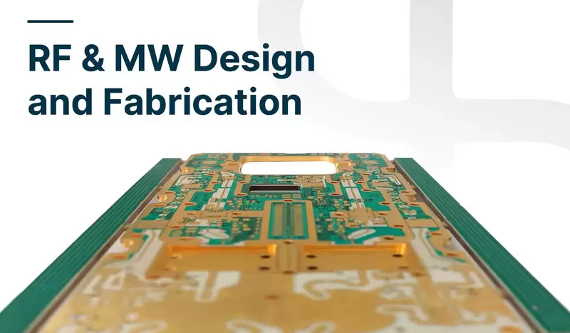
PCB Design for Radio Frequency & Microwave solutions
Learn about our advanced PCB design solutions offering high-performance Thermal Management options for Radio Frequency & Microwave applications.

PCB Thermal Management Solutions
As electronic devices pack more power into smaller spaces, heat generation can prove to be a major setback

iNPACK™ Panel Level Solutions
Learn about iNPACK™ advanced Panel Level Solutions, which offer high performance & utilizing an exceptional packaging process

Miniaturization: The New Frontier in Aerospace
See the many exciting new miniaturized technologies transforming the Aerospace and Space Robotics industry.

An In-depth Look at Wire Bonding Options
See the many exciting new miniaturized technologies transforming the Aerospace and Space Robotics industry.

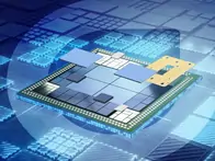
Die Stacking Technology in PCB Design & Manufacturing
Die Stacking Technology, also known as 3D Stacking, opens the door to a world of advanced packaging possibilities.

SiP Reliability Analysis & Testing
There are significant performance, functionality and form factor improvements with System-in-Package (SiP) technology - formulas included

X-VIA Technology: Critical for HDI Packages
Critical for HDI packages and thermal management of heat sensitive electronics, see how X-VIA technology comes into play.

The Time is Now: Antenna-In-Package (AiP) Solutions
RF system designers know that Antenna-in-Package (AiP) technology can provide a superior solution.

Multi-chip Modules & System-in-Package Technologies
MCM & SiP Technologies - Moving Us Forward On the ‘More than Moore’ Road Map

Why Introduce Graphene into Advanced PCBs?
Why Graphene Attracts Advanced PCB Designers? High electron mobility, X100 faster than silicon, conducts heat like diamonds, superior electrical conductivity to Cu, are just some examples.

Focusing on Substrate PCB
Simply put, substrate PCB are the core support material for IC packaging. They function as a mechanical structure, as well as an electrical interconnect for one or more devices

When is a Miniaturized PCBA the Right Option for You?
Explore Miniaturized PCBA Design, the benefits and options; space optimization, power efficiency, thermal management, enhanced signal integrity and more

The Complexities of Microelectronics Microwave Modules
Microwave and millimeter-wave frequency package design requires a special kind of expertise. It’s a far more complex process than working with lower frequencies.
‘Moore’ than a PCB – Breakthrough Solutions
Discussing breakthrough solutions for the challenges facing the semiconductor and microelectronics industry.

What mSAP Technology Can Do for Your Advanced Applications
Learn about mSAP Technology; exploring its huge growth potential impact on the design, fabrication & manufacturing processes.

SLP – Substrate-Like PCB Technology
Learn about SLP Technology; exploring its huge growth potential impact on the design, fabrication & manufacturing processes.

Substrate – Miniaturization & Special Design Rules
Watch our Webinar which will discuss what needs to be considered when designing a Miniaturized Substrate.

Advanced miniaturized solutions - from design to manufacturing
All-in-One | From design to manufacturing of advanced miniaturized solutions

Extreme heat dissipation solution in PWB stage
Extreme heat dissipation solution in PWB stage

PCB Extreme heat dissipation solution in PWB stage | Case study
Extreme heat dissipation solution in PWB stage | Case study

Innovation at its best – Packaging solutions at the COMCAS conference
Yaniv Maydar, PCB Technologies V.P. of R&D and Innovation, attended COMCAS, one of IEEE's prime conferences, held in Tel-Aviv.
Far east PCB, PCBA and Box Build - Original poster
Far east PCB, PCBA and Box Build at competitive prices under end-to-end responsibility of PCB-Technologies

In-house HATS lab- Evaluating reliability for extended survivability
In-house HATS (Highly Accelerated Thermal Shock) lab- Evaluating reliability for extended survivability

Enhanced capacity for precise and speedy production
Our newest addition – the advanced #Excellon’s Cobra #laser system featuring UV and CO2 laser capabilities, helps us meet this challenge.

All-in-One – the lab inspection angle
All-in-One – the lab inspection angle | PCB News

PCB Technologies Launches iNPACK, a Miniaturization, and Advanced Packaging Solution Provider
PCB Technologies Launches iNPACK, a Miniaturization, and Advanced Packaging Solution Provider

All-in-One Substrates and Advanced Packaging Solutions
All-in-One Substrates and Advanced Packaging Solutions | PCB News

mSAP boosts HDI PCB capabilities
Modified Semi Additive Process (mSAP) boosts High-Density Interconnect (HDI) PCB capabilities
Our new CU fill machine enabling ESP
Our new CU fill (electroplated) machine enabling enhanced system performance

How can you ensure your customer a QTA (Quick Turn Around)
When it comes to QTA projects of prototype or low/mid volumes production, we stick with parallel (as opposed to linear) workflow.

Miniaturization – The main challenge
Miniaturization – special laminate materials and buried capacitors technology in the works

Miniaturization technology – Controlling thermal expansion and power dissipation
To ensure system reliability and space reduction, the package should comply with several thermal, mechanical, and electrical requirements

The best of both worlds
The competitive, fast-track market in which electronic device designers operate compels us to develop out-of-the-box solutions

Why just dense when you can miniaturize?
The High Density substrate in the picture is based on a unique production technology. A four stack up layered PCB in total height of 260 – 300 µm.!

Test and Inspection Management
Hardware design and manufacturing of new electronic devices entail end-to-end quality inspection processes to ensure the delivery of defect-free products and systems

Solid data management – key to accurate quotes
When it comes to pricing, the impact it holds on the profitability of any company is even more crucial. PCB Technologies utilized SAS’ JMP statistical software supporting its customers’ need for a quick, reliable quote.

New miniaturization technology
Miniaturization compels us to constantly look for and implement new technologies.

Supporting Semiconductors machine manufacturers
The semiconductor’s supply chain’s delays we have been accustomed to ever since the COVID19 era began and their effect on the lives of people all over the world are accelerating.
To get the file, fill in your Email
Thank you
We will contact you shortly