PCB Fabrication: Subtractive vs. mSAP
Yaniv Maydar
|21st May ,2024
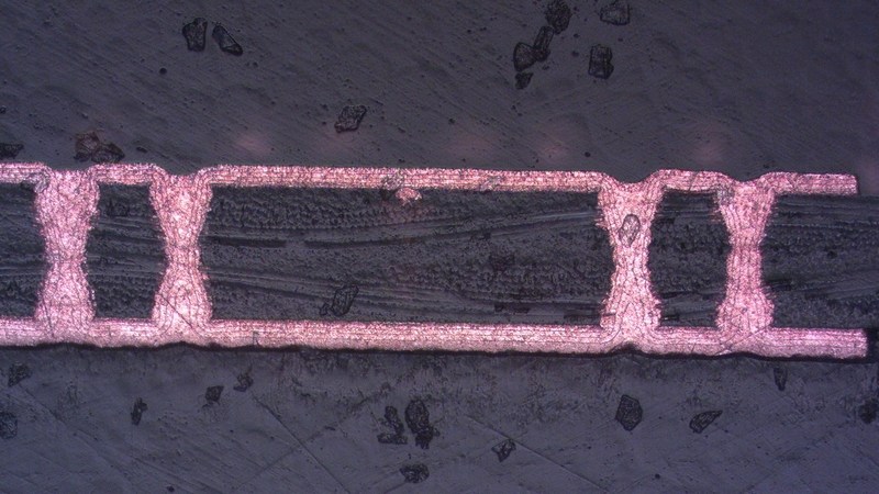
While both Subtractive and mSAP processes use photolithography to define circuit patterns, differences lie in how each process handles material removal and any further fabrication steps required to complete the PCB. mSAP for instance, incorporates additional additive steps to achieve finer, more precise control over circuit features compared to subtractive photolithography, allowing for denser circuits and better control over impedance, which is crucial for high-speed circuits. Subtractive photolithography however, is a mature and widely used process, while mSAP is a newer technology that currently demand higher costs.
You’ll want to carefully consider design complexity, electrical performance, production volumes and budgetary constraints, when choosing between Subtractive Photolithography manufacturing and the Modified Semi-Additive Process (mSAP).

See also: PCB Solutions, 3D IC packaging
Process Steps:
|
Subtractive Process |
mSAP Process |
|
|
mSAP Key Advantages:
The additive aspects of the mSAP process, allows for more precise control over circuit features; achieving finer feature sizes, improved accuracy and reduced material waste. These capabilities are especially advantageous in manufacturing high-density interconnect (HDI) PCBs.
Process Features:
- Fine Pitch & High-Density Traces: mSAP enables the creation of finer and higher-density circuit traces. This is crucial to accommodate PCB designs that require densely packed components.
- Accuracy & Resolution: mSAP enables greater control and precision in defining circuit patterns. This becomes a crucial issue when designing for more complex and miniaturized electronic devices.
- Signal Integrity: The ability to create finer traces and spacing using mSAP technology, allows for improved signal integrity. This is especially important for high-frequency / high-speed electronic applications, here reduced crosstalk and optimal impedance control are critical.
- Thinner Dielectric Layers: mSAP allows the use of thinner dielectric layers between copper traces. These thinner dielectrics contribute to overall miniaturization and are essential in applications with space constraints.
Important Benefits:
- Less Material Wastage: Unlike traditional subtractive processes that entail etching away excess copper, mSAP selectively adds copper only to the areas where it’s needed. This results in less material wastage, making the process more environmentally friendly and cost-effective.
- Reliability & Consistency: Enabling more precise control in the fabrication process with mSAP, leads to higher levels of reliability and consistency in the final product. This becomes critical in applications such as aerospace and medical device, where reliability is of paramount importance.
- Added Value: Although the initial setup costs for mSAP may be higher than with subtractive processes, for certain applications it can actually be more cost-effective. mSAP technology is proving to be the better option for high-volume production of advanced PCB designs. Adding to that it’s inherent ability to reduce material waste, can translate into notable cost savings.
- HDI Compatible: mSAP is well-suited for manufacturing High-Density Interconnect (HDI) boards. mSAP facilitates the kind of intricate circuitry HDI designs require in order to incorporate multiple layers of copper traces and vias within very tight spaces.
Subtractive Photolithography Key Advantages:
The Subtractive process is a well-established method of producing high-quality PCBs and microelectronics. While newer processes like mSAP offer certain advantages, subtractive photolithography is considered the industry standard, applicable for a wide range of PCB designs, from simple single-layer PCBs to more complex multilayer boards.
Production Advantages:
- Industry Standard: Most manufacturers are long-experienced in using subtractive processes, and have the infrastructure to support it; including etching equipment and waste disposal systems.
- Relatively Simple Setup: subtractive photolithography typically involves a simpler setup than other more advanced processes, facilitating rapid prototyping and quick production turnaround.
- Material Compatibility: Subtractive technology can handle processing a wide variety of materials, including different types of metals and dielectric materials. This flexibility can accommodate PCB designs with diverse material requirements.
- High Throughput: Subtractive processes can often achieve very high throughput and are well-suited to large-scale production. Familiarity with the Subtractive process and the infrastructure to support it, enables a smoother, more efficient manufacturing workflow.
- Cost-Effective: All of the benefits mentioned above contribute to the popularity of Subtractive processes as a cost-effective method of production for a wide range of PCBs, especially where high precision or fine detail is not critical.
Comparison: Subtractive vs. mSAP
While subtractive photolithography remains a viable production method for many applications, it’s essential to weigh-up factors such as design complexity, precision requirements and budget when making a choice. A more complex fabrication process, like mSAP, is usually preferred in applications demanding high-density circuits, fine pitch traces or other advanced features; not seen as practical or cost-efficient with subtractive methods alone.
|
Feature |
Subtractive |
mSAP |
|
Process |
Starts with full copper, defines pattern |
Starts with thin copper seed, |
|
Upside |
Mature technology, cost-effective |
Finer features down to 25 microns, |
|
Downside |
Larger features, over 75 microns, complex process, generates waste |
Newer technology, potentially more |
|
Best for |
Simpler designs, lower volume |
Complex designs, fine features, high volume (with established mSAP capability) |
So, What’s The Best Option?
The choice between subtractive photolithography and mSAP mainly depends on specific design requirements for the PCB. Subtractive photolithography remains a popular method for many applications due to its established use and lower cost. However, mSAP is gaining ground fast for high-density, high-performance PCBs.
PCB Technologies, where cutting-edge technology meets advanced manufacturing processes. Our All-In-One capabilities, means everything at is done under one roof: PCB Substrate, Microelectronics, IC Packaging, PCBA, Box Build, Testing & more. Our expert tech team is always available, so feel free to consult with us to choose the best range of processes for your project requirements.