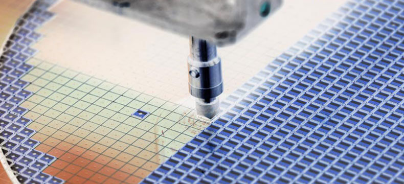
Critical Applications for the Semiconductor Sector
PCB capabilities that can deliver a combination of high reliability, speed and density are essential in mission-critical applications where semiconductor failure is not an option; Aerospace, Defense, Avionics, Advanced Med-Tech, Autonomous Automotive, etc.
Supporting AI & HPC Technologies
Semiconductor PCBs function as a fundamental enabling technology for ultra-fast data transmission in AI technology and High-Performance Computing (HPC) data centers, by dictating ultimate speed, power efficiency and reliability of accelerators (like GPUs and ASICs) and the servers they populate.
These chips have massive, transient power demands (often >700 W with 100 A currents) as billions of transistors switch simultaneously. Therefore, the PCB Power Delivery Network (PDN), must maintain a stable supply voltage with minimal ripple or voltage droop to avoid errors.
Proper performance hinges on handling three main technical challenges at high-speed frequencies (i.e. GHz or over): Signal Integrity (SI) / Power Integrity (PI) / Thermal Management. Ultra-fast data transfer like DDR5 memory at up to 6.4 Gbps or PCIe 5.0 interconnects, is achieved by PCBs able to minimize signal degradation across high-frequency transmission lines.
Unique Technological Know-How & Solutions
System-in-Package (SiP) Solution: The heterogeneous integration of separately manufactured components into a higher-level assembly, SiP is able to leverage the advanced capabilities of packaging technology by creating a system close to the System-on-Chip (SoC) form factor but with better yield, lower overall cost, higher flexibility and faster time to market. Various technologies can be used in SiP design, interconnect technologies (vertical and horizontal), encapsulation technologies (protection and stabilization), and packaging architectures. The number of available technologies for SiP implementation is growing rapidly.
Multi-Chip Modules (MCMs): Differences between MCM and SiP technology are mainly in their respective scope and functionality. The MCM is an electronic assembly that integrates multiple integrated circuits (ICs) and other components onto a single substrate to function as one larger, more powerful unit. MCMs lead to improved performance, higher density and miniaturization by reducing interconnect lengths and allowing for the integration of different semiconductor technologies in a single package. They differ from System-in-Package (SiP) by typically representing a tightly coupled subsystem rather than a complete system.
Technical & Performance Imperatives
The technical prerequisites listed below are non-negotiable across a diverse range of high-stakes applications, including Advanced Driver-Assistance Systems (ADAS) in automotive electronics, avionics & satellite communication systems in aerospace, infrastructure for 5G/6G technologies and critical monitoring/imaging equipment in the medical sector. PCBs within the semiconductor industry are subject to exceptionally stringent performance metrics, with advanced interconnect solutions that must deliver:
- Extended Functional Integration: Facilitating sophisticated system-on-a-chip (SoC) architecture and complex multi-die integration.
- Mass Reduction & Power Efficiency: Achieving ultra-lightweight designs concurrently with minimized power consumption (P-dissipated) to optimize thermal management and overall system efficiency.
- High-Fidelity / High-Volume Data Transmission: Ensures the integrity and speed of data signals across interconnects, capable of supporting multi-gigabit per second (Gbps) transfer rates with minimal signal integrity (SI) degradation, including crosstalk and reflection losses. Critical for meeting latency and bandwidth requirements of modern digital processing and communications systems.
- Reliability & Longevity: Maintaining robust performance under varied operational stresses, including thermal cycling, mechanical vibration and high-frequency electromagnetic interference (EMI).
Strategic Manufacturing & Fabrication Expertise
High-Density Interconnect (HDI) & Miniaturization: HDI PCBs are characterized by a significantly higher wiring density per unit area than traditional PCBs. Utilizing advanced dielectric materials with optimized Dk (dielectric constant) and Df (dissipation factor) for superior high-frequency performance. Key design and manufacturing features include:
- Micro-Via Technology: Tiny, laser-drilled holes (≤0.15mm in diameter) used to connect layers. They allow for finer pitch components and more routing in a smaller area. More advanced forms, known as Ultra-HDI (UHDI), push feature sizes to the extreme with micro-vias as small as 2mils (50µm).
- Blind & Buried Vias: Vias that don’t pass all the way through the board (blind) or that connect internal layers only (buried) are used to free up valuable routing space on the surface layers.
- Fine Lines & Spaces: The use of advanced processes like modified Semi-Additive Process (mSAP) enables finer trace widths (≤0.1mm or 4mils), allowing for more circuitry and greater component density.
- Controlled Impedance Trace Design to ensure characteristic impedance matching for high-speed differential pairs, thereby preserving signal integrity and minimizing Bit Error Rate (BER).
- Role in Semiconductors: High density is crucial for connecting to complex semiconductor packages, such as Ball Grid Array (BGA), Chip Scale Packages (CSP), and Wafer-Level Packages (WLP), which have massive numbers of I/O connections (pins) in a tiny footprint.
High-Speed Performance & Signal Integrity: As semiconductor devices handle ever-increasing data rates, the PCBs they connect to must support high-speed signal transmission without degradation.
- Signal Integrity (SI): HDI PCBs are designed to minimize signal loss, crosstalk and impedance mismatches. Shorter interconnection paths, made possible by micro-vias, reduce parasitic capacitance and inductance; vital for maintaining clarity and timing of high-frequency signals.
- Advanced Materials: Specialized, low-loss dielectric materials are essential. They have a low dielectric constant (Dk) and low dissipation factor (Df) to reduce signal attenuation and maintain controlled impedance, chiefly for 5G, cloud computing, AI accelerators and other high-frequency applications.
- Thermal Management: High-performance ICs generate significant heat. HDI and UHDI PCBs incorporate features like thermal vias and use materials with good thermal stability to efficiently dissipate heat; crucial for long-term device performance and reliability.
When you think miniaturization, think iNPACK (A PCB Technologies Division):
Experts in organic substrates and enhanced micro-electronics packaging technologies, iNPACK focuses on high-end technology that helps improve signal integrity and reduces unwanted inductance effects. We provide SiP, semiconductor packaging, organic substrates (25-micron lines and 25-micron spacing) and 3D, 2.5D, and 2D packaging solutions, to many of the world’s most demanding industries.
Our unique design & assembly processes achieve high-level, customized results with IC packaging solutions tailored to customer applications. We offer the design freedom to choose from a variety of custom options perfectly aligned with your project needs: Antenna-in-Package, Flip-Chip, QFN package technology, Filter-on-Package and more.
iNPACK delivers comprehensive substrate panel-level manufacturing and engineering support to our customers across the board; in fact, they depend on it. Contact our experts anytime to discuss your project needs.