
Industry 4.0 & Beyond
The ‘Industry 4.0 Digital Revolution’ signifies a profound transformation within manufacturing and industrial processes. It’s powered by a suite of interconnected technologies that drive ‘smart’ systems, hyper-automation and data-driven decision-making at unprecedented speeds. Primary Industry 4.0 capabilities stem from this fusion of technologies, allowing for intelligent systems across various sectors; such as Autonomous Robots, Big Data and the Industrial Internet of Things (IIoT).
Smart Reliance on PCBs: To support the precision and connectivity that new-wave automated industrial applications demand, smart factories require dedicated electronics (machinery and equipment), enabled by advanced PCB technology.
For Today’s Electronics & Future Innovations:
Soft Robotics/Wearable Electronics: Using Flexible & Stretchable PCBs to enable conformable, bio-integrated robotics, like soft grippers or wearable exoskeletons that require non-planar electronics.
Additive Manufacturing (3D Printing): Using 3D-Printed PCBs for new or non-traditional circuit geometries with rapid prototyping; potentially integrating electronics directly into the product structure.
Artificial Intelligence (AI) at the Edge: PCBs with Integrated AI Accelerators, that incorporate complex, thermally managed boards to run machine learning models directly on factory floor equipment; for immediate decision-making, as with real-time visual quality control.
Advanced Traceability: PCBs with Embedded Traceability Codes. Miniaturized barcodes or RFID tags integrated into the PCB layers for end-to-end tracking of every board; enabling quality control and predictive maintenance.
Industry 4.0 Applications
PCBs are embedded in virtually every component of the smart factory ecosystem, enabling interconnected, autonomous, real-time operations for key applications:
- Advanced Industrial Robotics (Robots and Cobots):
- Real-Time Motion Control: Multi-layer and High-Density Interconnect (HDI) PCBs house high-performance processors and motion control drivers, crucial for real-time communication protocols like EtherCAT or PROFINET, for precise, coordinated robotic movements.
- Sensor & Actuator Interfacing: To connect and manage an impressive array of embedded sensors, for torque, position, force feedback and actuators (servo motors).
- Flexible Circuits in Articulated Arms: Flexible (Flex) & Rigid-Flex PCBs are used in joints and articulated sections of robotic arms. Allows high-cycle bending while maintaining signal integrity and reducing overall weight and size of the arm.
- Smart Sensors & Industrial IoT (IIoT) Devices:
- Miniaturization: HDI PCBs with Micro-vias and component embedding technology are essential for creating the small form factors required for IIoT sensors, fitting into constrained spaces on machinery or assembly lines.
- Edge Computing: Integrating low-power microprocessors to perform local data processing and filtering at the sensor level; reducing latency and data volume sent to the cloud.
- Connectivity: Supporting various wireless communication modules (Wi-Fi, 5G, LoRa) and managing the high-frequency signals required for reliable data transmission in crowded industrial environments.
- Autonomous Guided Vehicles (AGVs) & Drones:
- Navigation & Control: Operation of flight-control and vehicle-control boards; integrating high-speed computation, inertial measurement units (IMUs), GNSS (Global Navigation Satellite System) receivers and motor control circuits.
- Lidar/Radar Modules: For Advanced Driver Assistance Systems (ADAS), housing the high-speed signal processing units for Lidar, radar, and machine vision cameras that enable obstacle detection and real-time mapping.
Demands for Specialized Industrial PCBs
PCB Technologies provide our customers in the industrial sector with advanced capabilities that meet the exacting demands of the digital industrial revolution. We offer PCB solutions directly responsible for helping to overcome the limitations of older automation systems, while also serving new-wave industrial needs.
- High-Density Interconnect (HDI) & Miniaturization: Smaller, more powerful electronics require HDI PCB technology for finer lines, tighter spacing and tiny connections (micro-vias), that increase component density; allowing for more complex control circuitry, processors and communication chips to be packed into less space.
- Durability in Harsh Environments: Industrial settings are often characterized by extreme conditions, (temperature, electronic noise, chemicals etc.), demanding extra durable PCB operation.
- Ruggedized Materials: PCB materials and laminates must withstand vibration, shock, dust, chemicals and wide temperature ranges (-40^ to 85^).
- Heavy Copper PCBs: Thicker copper layers used for high-power applications, such as motor control or power supplies. Heavy Copper PCBs manage high currents (up to 100A or more), acting as natural heat sinks to dissipate heat.
- Signal Integrity & Speed: Elevated data rates for real-time control and vision systems require high-frequency PCBs using materials with low dielectric loss to ensure minimal signal loss, interference or distortion at high frequency transmission (above 1 GHz).
- Controlled Impedance: PCB design must ensure that characteristic impedance of transmission lines (traces) is precisely controlled (~ 50 ohms) preventing signal reflection, noise or data corruption in high-speed protocols.
- EMI Shielding: Multilayer PCBs and specialized routing techniques provide robust electromagnetic interference (EMI) shielding, enabling clean signals in electrically noisy factory settings.
Our Role in the Industrial New Wave
Industry 4.0: The Digital Revolution / Industry 4.5 The Transitional Concept / Industry 5.0 The Human-Centric Revolution: These terms describe the proposed evolution of industrial production; moving from technology-driven automation alone, to a more human-centric and sustainable future for industry.
PCB Technologies is dedicated to the continued drive for innovation in PCB materials and manufacturing; cementing our role as an indispensable foundational technology company for the future of advanced industrial automation, smart systems and beyond.
Contact us to discuss your project needs for today and tomorrow.
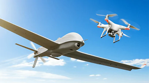
UAV PCBs
Unmanned Aerial Vehicles (UAVs) are primarily categorized by design and flight dynamics into fixed-wing, rotary-wing and hybrid types. All are driven by sophisticated electronic technologies in propulsion, autonomous navigation, flight control and include onboard high-speed data processing, long-range communications and specialized sensors. These various components must operate flawlessly within strict size, weight and power constraints and often in extreme environments.
UAV or Drone applications include Search & Rescue Missions, Critical Infrastructure Inspection, Military Maneuvers, Scientific Research, Agricultural Management, Autonomous Delivery Logistics and many others.
UAV Deep Integration of Components:
- Specialized Sensors: Optical, thermal, and multispectral cameras, LiDAR, and specific gas or chemical detectors.
- High-Speed Communication: Robust radio frequency (RF) systems and high-bandwidth optical communication technologies to ensure data transmission stability and speed.
- Embedded Systems: Onboard computers and microcontrollers for flight control, navigation and data acquisition.
- Power Management: Efficient power distribution and high-density battery systems (or alternative power sources like fuel cells) to maximize endurance and payload power.
PCB Capabilities Enabling UAV Electronics
Whether for commercial purposes or critical stealth missions, PCB Technologies focus our capabilities on enabling maximum efficiency, reliability and versatility for UAV operations. The electronics that drive UAV functionality demand expertise in miniaturization, ruggedization and high-performance signal integrity.
|
Technology |
Rationale for UAV |
Benefit |
|
High-Density Interconnect (HDI) PCBs |
Crucial for miniaturization, HDI technology features finer traces, micro-vias and higher layer counts; allowing more components to be packed into a reduced footprint. |
Significantly aids in weight reduction and compact design; essential for extended flight times and better maneuverability. |
|
Rigid-Flex PCBs |
Combines the durability of rigid boards with the flexibility of flexible circuits, allowing the PCB to bend and fold to fit into irregular, space-constrained areas within the Drone. |
Reduces the need for bulky connectors and cables, enhancing overall system reliability by minimizing potential failure points in high-vibration environments |
|
Advanced & |
UAVs need reliable communication and sensor performance, often at high frequencies (above 1 GHz). This requires special materials like polyimide or PTFE/Rogers laminates for stable dielectric constants (Dk) and low dissipation factors (Df), across wide temperature ranges. |
Effectively minimizes signal loss and ensures signal integrity even under harsh conditions. |
|
Thermal Management Solutions |
High-power electronics generate considerable heat. Countermeasures include thermally conductive substrates and special design features like thermal vias and copper pours. |
Prevents overheating and ensures component longevity along with reliable performance in demanding environments. |
|
Robust & Shielded Designs |
PCBs for UAVs must be adapted for harsh or rugged environments by use of stronger materials, strategic component placement, conformal coatings and dedicated ground planes/shielding. |
Ensures the ability to withstand extreme temperatures, shock and vibration, protects against moisture and corrosion and mitigates Electro-magnetic Interference (EMI). |
Advanced PCB Miniaturization Enables More Efficient Flight Missions
- Resource Optimization: Miniaturized systems integrate more mission-critical components packed into smaller spaces: sensors, wireless communication, control units, power generators etc. Boosts payload efficiency, reduces power losses, and better supports thermal management.
- Reliability & Flexibility: Integrating multiple microsystems into a silicon wafer and redundancy by design, increases reliability and flexibility. Smaller, more reliable systems reduce operating risks associated with complex flight missions, especially in harsh environments.
- Cost Reduction: Miniaturization reduces payload mass and volume, enabling more ambitious flight missions with increased agility, maneuverability and precision. Optimized performance results in lower costs across the entire system.
- iNPACK a PCB Technologies Subsidiary: Providing advanced semiconductor and electronics assembly, testing, IC package design, plus LGA, BGA and 2D & 3D customized solutions. MW microelectronics assemblies, System-in-Package (SiP), heterogeneous integration and much more.
PCB Technologies — Pushing the Boundaries of Drone Technology.
We Provide Custom Solutions for Drone Technology, Counter-UAV Systems & Prototyping.
A UAV or Drone PCB is not simply a substrate for electrical connections, but a mission-critical component, responsible for the overall reliability of the system. For that reason, we make sure that our PCBs enabling UAV technology fully support functional stability and flight efficiency, with no-fail operation.
As UAVs become increasingly independent, complex and application-specific, their underlying electronics must also evolve. PCB Technologies address this issue by positioning ourselves as vital partners in the evolutionary process; enabling optimal UAV and Drone performance, durability and innovation.
Defending Against Threats: Counter-UAV Systems
PCB Technologies empowers defense industries to master electronic warfare challenges. We specialize in thermal management, EMI compliance, and miniaturization for combat UAV countermeasures such as: laser systems, missile defense, and high-powered microwave solutions. Our unique heterogeneous engineering approach delivers peak performance in extreme environments.
Prototyping UAV PCB Designs for Success
- Ensures PCB design and functionality measures-up to the specific UAV or Drone application required (especially for experimental models).
- Prototyping is a highly practical method of validating design concepts, by identifying and correcting potential issues before they occur; like inadequate thermal management, power distribution errors or structural weaknesses.
- When you’re talking about industries like defense/military and aerospace, any compromise in product quality poses a critical risk, therefore prototyping isn’t just a convenience, it’s a necessity.
Let’s discuss your UAV project requirements. Our experts are available at your convenience.

Sensor Technology
From medical diagnostics and industrial automation, to far-flung space exploration, the success of today’s sensor technologies ultimately hinges on the quality of the PCB Design and Fabrication processes invested in producing them.
Sensor Ecosystems – includes flow, image, level sensors, light, motion, positioning and temperature sensors to name a few. Although extremely varied in functionality, they all rely heavily on-data transmissions and analysis gathered from the environment, manufacturing assets and specialized equipment.
Designing PCBs for Sensors – requires meticulous, complex disciplines that factor-in numerous parameters: Environmental influences impacting operation, Form Factor, Power Requirements and Signal & Power Integrity, that can make or break reliability and repeatability for critical (no-fail) applications.
Cost & Efficiency – Expertise in substrate design plus advanced FAB facilities (equipped with best-in-class Film Assisted Molding Machines), produce a wide range of Microelectronics, System-in-Package Solutions and high precision miniaturized sensors, with minimum trace spacing and width. Our common design rules (PCB, Substrate & Packaging) all under one roof, provide high-efficiency services that boost quality, reduce time to market and lower costs.
What Does Sensor Packaging Entail?
It’s is a complex form of integrated circuit (IC) packaging that integrates sensors with other components to perform specific functions; requiring electrical connections, structural protection and environmental interfaces.
Key Innovation: MEMS technology enables miniaturized, high-sensitivity sensors, while advanced techniques such as System-in-Package (SiP) and 3D IC stacking allow for the heterogeneous integration of various components into a single, unified package.
Safe-Keeping: Sensor packaging must offer protection from exposure and harsh operating conditions; extreme temperatures, vibrations and corrosive environments. This requires specialized materials and custom design processes to ensure continuous reliability and functionality.
Driving Force: We keep up with rapidly evolving sensor technology by devoting our strategic resources to R&D, as well as investing in advanced manufacturing processes, material sciences, miniaturization, and all-around sensor integration with newer technologies; namely AI, IoT and machine learning.
Types of PCB Sensors
- Temperature Sensors convert temperature changes into electrical resistance/voltage signals (Thermistors, RTDs, Thermocouples). Applications include: HVAC systems, CPUs, battery packs, industrial machinery.
- Pressure Sensors convert pressure into electrical signals to monitor gas or liquid pressure. Applications include: Automotive systems (e.g., tire pressure monitoring), medical devices, industrial automation.
- Motion & Acceleration Sensors measure linear acceleration or angular velocity and function as motion detectors, such as accelerometers and gyroscopes. Applications include: Smartphones, fitness trackers, wearables.
- Gas & Chemical Sensors detect various gases (e.g., carbon dioxide, carbon monoxide, methane, nitrogen dioxide). Applications include: Safety systems, environmental monitoring, smart homes, laboratories or industry.
- Humidity Sensors are embedded in PCBs when accurate environmental readings are necessary. Applications include: Weather stations, agricultural systems, air conditioning systems.
- Light Sensors also referred to as photodetectors, are designed to gauge ambient light intensity. Applications include: Smartphones, streetlights and solar applications for dimming or solar tracking.
- Touch and Proximity Sensors detect physical touch, or the proximity of an object, without actually touching it. Applications include: Robotics, touch screens and smart appliances.
About Us
PCB Technologies is uniquely positioned to offer our advanced design and fabrication capabilities for life-changing Microtechnology applications; specifically, BioMEMS & Sensors; essential in the production of so many new and exciting electronics being introduced into industrial processes and science-based disciplines worldwide.
Along with cutting-edge machinery, PCB Technologies also have the technical power. Our top-tier in-house engineering team is dedicated to supporting customers every step of the way; especially during the crucial early-stage design process.
As an All-in-One PCB Solutions Provider, we cover the entire product development process (all under one roof), making it simpler and easier for our customers to reach their project goals at a reduced time to market and with significant cost savings.
Let’s talk Sensors, Contact Us.

Antenna-in-Package (AiP) Technology
PCB Technologies answers top-priority challenges for RF systems requirements by offering innovative System-in-Package (SiP) solutions, such as Antenna-in-Package (AiP) technology, to help Reduce Size, Weight, Power & Cost (SWaP-C), while also maintaining or even enhancing overall system performance.
AiP is an ideal solution that integrates one or more antennas directly into the same integrated circuit (IC) package as the RF transceiver chip, replacing traditional methods of placing antennas as separate components on or near the main PCB. This compact configuration, often utilizes flip-chip ball grid arrays and a package substrate; simplifying the design process; especially for millimeter-wave (mmWave) applications.
Key Advantages of AiP
- Miniaturization & Space Savings: Placing the antenna and RF chip in a single package creates a much smaller form factor, which is essential for compact devices.
- Enhanced Performance:
- Reduced Signal Loss: A shorter interconnection between the antenna and the RF chip minimizes signal attenuation and improves signal integrity.
- Better Thermal Performance: The integrated design more efficiently dissipates heat and extends system longevity than conventional configurations.
- Improved Security & Resilience: Integrated package provides higher security levels against unauthorized access or tampering and is more resilient to harsh environmental factors like moisture or heat.
- Simplified Manufacturing: Integrating the antenna and RF chip into one package reduces the number of components and assembly steps; streamlining the production process.
- Design Flexibility: AiP technology and can be combined with other System-in-Package (SiP) technologies to house front-end components like power amplifiers, low-noise amplifiers, filters and switches within the same package, forming a complete antenna module.
Optimal Frequencies for AiP
Well-suited for high-frequency applications where antenna dimensions can fit within an IC package.
- Wavelength and Antenna Size: The size of an antenna is directly related to the wavelength of the signal. At higher frequencies, the wavelength is shorter, allowing for smaller antennas.
- 1 GHz: Wavelength (λ) is 30 cm.
- 10 GHz: Wavelength is 3 cm.
- 100 GHz: Wavelength is 3 mm.
- Millimeter-Wave (mmWave) Spectrum: The mmWave spectrum (30-300 GHz), also known as the Extremely High Frequency (EHF) band, is the ideal fit for AiP. The small wavelengths (1-10 mm) allow for antennas that can be easily integrated into a package.
- Other Frequencies: While mmWave is optimal, AiP is also used in the 1-30 GHz range.
Typical AiP Applications
The advantages of AiP have led to its rapid adoption across a wide range of industries and applications where size and weight constraints are critical, including:
- 5G Mobile Networks: AiP is a perfect fit for 5G mmWave devices, as the smaller antennas required can be directly integrated into the package. It also supports the MIMO (Multiple In/ Multiple Out) antenna configurations needed for 5G diversity.
- Automotive Radar: AiP is widely used in 77-GHz automotive radar systems.
- Wireless Communication: It’s used in WiFi routers, wireless sensor networks, and high-frequency radios (e.g., 60-GHz gesture radar).
- Medical & Defense: AiP is found in medical imaging and military & defense equipment, due to high performance attributes and security benefits.
- Miniaturized / Compact Electronics: Drones, wearables. smartphones, medical devices, robotics, smart-home systems and more.
Potential Limitations
Although powerful, AiP technology isn’t suitable for all RF designs. Because RF components and antenna elements are modeled as a single unit, not individually, special efforts in up-front design, planning and implementation are necessary. Frequencies, thermal issues, RF power, DC power and other design aspects must be factored in, which may require special expertise for successful implementation.
What’s Next?
iNPACK offers a wide range of In-Package systems for high-frequency applications: From 60 GHz for radio, automotive radar, phased arrays, advanced sensors etc., and from 20 GHz up to 100 GHz for special applications. Have a question? Get in touch with one of our experts about your AiP design needs now.

Electro-Optic PCBs
With the rapid adoption of cutting-edge sensors, laser systems and imaging solutions, Electro-Optic (EO) instrumentation technology has become a cornerstone of innovation, leading unprecedented precision, efficiency and data processing capabilities throughout a vast range of industries.
TRENDING NOW: New-Tech Applications for Defense, High Speed Cameras & Autonomous Vehicles Feature Advanced Electro-Optic Instrumentation.
- Thermal Optic Devices for Defense: Enabling advanced sensors in detecting infrared (IR) radiation (heat signatures) emitted by objects. This technology is critical in providing super-accurate night vision, boosting situational awareness and enhancing target acquisition and engagement where visible light is absent or obscured; creating a real tactical advantage across ground, air and naval forces.
- High Speed Cameras for QA Processing: ‘Machine Vision’ solutions rely on electro-optics to enable components that acquire, process and interpret visual data for tasks that need speed, accuracy and consistency beyond human abilities: Used in Quality Control & Inspection, Measurement & Metrology, Guidance & Positioning (robotics), Identification & Tracking, plus Medical & Scientific Imaging Systems.
- Autonomous Vehicles (AVs): Electro-optic instrumentation technology is fundamentally used in AVs for environmental perception, navigation and safety systems through a suite of advanced sensors like LiDAR, cameras and thermal cameras. These optical systems act as the “eyes” of the vehicle, capturing data used by onboard computers and AI algorithms to make real-time driving decisions.
Enabling The Enablers
PCB design and manufacturing processes constitute the fundamental power and brains enabling this technology through high data rates, miniaturization capabilities, improved signal integrity and thermal management solutions. In addition, sophisticated design strategies, the use of specialized materials, plus high-precision fabrication and validation methodologies have been key factors in driving innovations like hybrid electro-optical PCBs; integrating both optical and electrical components.
More Electro-Optic Applications
At PCB Technologies we provide the foundational platforms that help enable electro-optics instrumentation to achieve greater speed, accuracy and reliable performance for our clients worldwide, across a range of complex and demanding applications.
- High-Speed Telecommunications: Electro-optic modulators (EOMs) encode vast amounts of data onto light beams at extremely high speeds (gigahertz frequencies) for transmission through fiber optic networks. They are fundamental to internet and data center infrastructure; meeting demands for fast, high-bandwidth data transmission that AI, big data processing and 5/6G networks require.
- Laser Systems: In laser technology, electro-optic effects precisely control the phase, amplitude and polarization of laser beams. This specialized technology is used in high-precision materials processing, advanced medical equipment (for eye surgery and cancer treatment), as well as laser printing and high-speed data recording.
- Sensing & Measurement: Electro-optic sensors are prevalent in industrial sectors like energy, civil engineering, defense and aerospace. They offer lossless transmission and high resolution in harsh or high-voltage environments, used in structural stress monitoring for bridges and dams, for satellites and space vehicles and in advanced night-vision / infrared systems for surveillance and defense.
- Optical Computing & Display Technologies: The ability to manipulate light with electricity is paving the way for next-generation computers that use photons instead of electrons for processing information, promising greater speed and energy efficiency. Electro-optics also play a part in new dynamically responsive display technologies.
- Optical Switching & Beam Steering: Used for optical routers and scanners, optical switching is the process of routing light signals from one fiber to another, while beam steering manipulates light beam direction for optical switching. Both technologies can be implemented using mechanical mirrors, galvanometer scanners, or phased-array optics and micro-mirrors.
Advancements on Demand
PCB Technologies provide advanced solutions to meet the exacting demands of electro-optic instrumentation. We offer engineering technologies and high-level manufacturing capabilities designed to enable even the most challenging projects in this technology sector.
Miniaturization & High-Density Interconnect (HDI):
- HDI allows for finer trace widths, smaller vias (blind/buried), and increased component density, enabling more compact and complex circuitry in electro-optic devices.
- Miniaturization is crucial for portable and space-constrained instrumentation, such as medical diagnostic tools, aerospace systems (drones, satellites) and wearable health monitors.
Advanced Materials & Optical Integration:
- The use of specialized low-loss materials like PTFE (Teflon) and Rogers laminates, instead of traditional FR4, minimizes signal loss and distortion at high frequencies; ideal for high-speed data transmission in electro-optics.
- Hybrid electro-optical PCBs (HEOPCBs) integrate optical waveguides such as embedded fiber optics, along with traditional copper traces onto a single substrate. This enables very high bandwidth communication (up to 100 Tbps or more per channel), overcoming bandwidth limitations of copper alone, while reducing the need for separate optical components.
Enhanced Signal Integrity & EMI Immunity:
- Design techniques, such as controlled impedance routing, dedicated ground and power planes, plus specific trace spacing, ensure signal quality while minimizing electromagnetic interference (EMI) and crosstalk.
- Optical signals, being immune to EMI, provide a significant advantage in mixed-signal electro-optical systems; leading to cleaner data transmission and higher reliability in noisy environments.
Effective Thermal Management:
- Electro-optic instruments often generate a significant amount of heat. Advanced PCB materials with high thermal conductivity, thermal vias and metal cores help dissipate heat efficiently, for more consistent, reliable product performance and longevity.
Precision Manufacturing & Testing:
- High-precision manufacturing processes, including laser direct imaging (LDI), automated optical inspection (AOI) and X-ray inspection, ensure scrupulous accuracy in layer alignment, component placement and solder joints.
- Rigorous testing and simulation, as in signal integrity analysis, (thermal analysis) during design and manufacturing stages, can catch flaws early, enabling far more reliable and durable instrumentation.
Consult With the Experts:
PCB Technologies is with you every step of the way, from initial PCB design, through fabrication, to full system integration. We bring to the table seasoned engineers with cutting-edge know-how, advanced PCB manufacturing processes and our dedicated iNPACK Division for expert miniaturization and IC packaging capabilities.
We’re also an All-in-One Solutions provider, ensuring a speedy transition from prototype to low/mid production volumes all under one roof. In this way, we keep a watchful eye on quality, cost and timelines, while you avoid the uncertainties of jobbing out to external vendors.
Let’s talk about how you can leverage our expertise.

Radar PCB Applications
Radar PCB design focuses on the need for dedicated materials coupled with specialized design expertise due to the very high-frequency microwave signals used in these systems. Basically, Radar systems operate by transmitting and receiving electromagnetic (EM) waves and calculating the travel time for these waves to bounce off objects, which in turn determines the distance to those objects. This functionality places stringent demands on the underlying PCB.
Airborne, grid, naval or land radar, phased-array, as well as Yagi-Uda radar PCBs, all combine various digital and mixed-signal technologies using very high-frequency microwave signals, which require exacting capabilities and a common design rules kit that PCB Technologies is able to provide.
High-Frequency PCB Materials
The most critical requirement for radar PCBs is the use of high-frequency (RF/Microwave) dielectric materials. Standard FR-4 materials are generally unsuitable because they introduce significant signal loss and variations at the microwave frequencies (typically 1 GHz to over 100 GHz) that radar uses.
Key Material Types Include:
- Polytetrafluoroethylene (PTFE) or Teflon: Known for its extremely low dielectric loss tangent (tanδ), which minimizes signal power loss, and a stable dielectric constant (ϵr) across a wide temperature range and frequency spectrum. This makes it a popular choice for high-performance radar.
- Ceramics: Often used in composite materials (ceramic-filled PTFE or hydrocarbon) or as purely ceramic substrates. They offer very stable (ϵr) and excellent thermal conductivity, which is crucial for managing heat from high-power components.
- Hydrocarbon Resins: These are often formulated into specialized laminates that provide a balance of high-frequency performance (low loss) and processing ease, sometimes acting as a lower-cost, high-performance alternative to pure PTFE.
Choosing the right material ensures the integrity of the microwave signal, enabling accurate measurement of EM wave travel time.
Design & Technology Integration
Radar PCBs are complex mixed-signal boards that integrate several distinct technology domains:
- RF/Microwave Front-End: This section handles the high-frequency transmit/receive path and includes components like power amplifiers (PAs), low-noise amplifiers (LNAs), mixers, and filters. This is where the specialized high-frequency materials are most critical, as signal traces must be designed as precise transmission lines (e.g., microstrip, stripline, coplanar waveguide).
- Analog/Mixed-Signal: This involves down-converting the high-frequency RF signal into an intermediate frequency (IF) or baseband signal, and then conditioning it using analog-to-digital converters (ADCs) and digital-to-analog converters (DACs).
- Digital/Processing Backend: This section, typically a high-speed digital board, houses the digital signal processors (DSPs) or Field-Programmable Gate Arrays (FPGAs) that perform the complex algorithms (like Fast Fourier Transform – FFT) to extract distance and velocity information from the digitized radar data.
Specialized Radar PCB Architectures
The principles apply across various radar implementations, requiring tailor-made design rules:
- Phased-Array Radars: These systems use an array of small antenna elements, where the phase of the signal to or from each element is individually controlled. This requires extremely tight phase and length matching on all transmission lines to ensure the antenna array can accurately steer and shape individual or multiple beams electronically.
- Yagi-Uda Radar PCBs: While less common for modern high-resolution systems, a Yagi-Uda antenna (a type of directional antenna) requires specialized transmission line design to connect to the PCB, often at lower frequencies or for simpler applications.
- Application-Specific Radars: The design must adapt to the operational environment, whether Airborne, Grid, Naval, or Land systems. For example, naval and land systems may have more robust environmental sealing requirements, while airborne systems prioritize weight and size constraints.
Key Design Expertise
Successful radar PCB design requires a specific “know-how” and adherence to specialized design rules kit; particularly concerning Signal Integrity (SI) and Power Integrity (PI) at microwave frequencies:
- Impedance Control: Precise control of transmission line impedance (typically 50 Ω) is mandatory. Any deviation can cause reflections, leading to signal loss and inaccurate measurements.
- Crosstalk Mitigation: High-frequency signals can easily couple between adjacent traces. Shielding, proper spacing and ground plane stitching are essential.
- Via Design: Standard through-hole vias can introduce significant inductance and capacitance at microwave frequencies. Low-inductance via designs, such as blind/buried vias and back-drilling, are often necessary to maintain signal quality.
- Layer Stackup: The PCB layer stack-up must be precisely engineered to achieve the required controlled impedance and to provide robust isolation between RF, digital and power layers.
- Thermal Management: Radar systems, especially those using high-power amplifiers (HPAs), generate substantial heat. Effective thermal design, utilizing thermal vias, specialized materials, and heatsink integration, is critical for component reliability and performance stability.
Consult with the Experts
PCB Technologies is a world leader in the design and manufacture of radar PCBs, including phased array air cavity antenna designs based on advanced semiconductor technology. Our next-generation capabilities address market demands for reduced size, weight and power consumption.
Utilization of a flat-panel approach, where each IC is easily mounted on the back of the antenna board, allows large-scale reduction of the antenna depth. The integration of higher frequency ICs (GaAs, GaN), makes advanced packaging and thermal management solutions a key factor in the production of phased array air cavities; reducing the physical size of the system. This improves long-term reliability, especially in multiple data stream radiation patterns. We also conduct complex testing protocols and inspection procedures to ensure full quality compliance.
PCB Technologies provides all-in-one solutions for high-reliability and mission-critical applications. Contact us to find out more.

MEMS Devices
Microelectromechanical Systems (MEMS) technology involves creating microscopic devices that integrate combined electrical and mechanical components (sensors, actuators and electronics) on a single silicon chip. These devices integrate a central processing unit (like a microprocessor) with components that interact with the physical world, primarily microsensors and micro-actuators. MEMS are fabricated using modified semiconductor manufacturing techniques, and range in size from one millimeter down to one micron.
Features & Advantages
- Miniaturization: MEMS devices are incredibly small (micrometers to millimeters), allowing for integration into compact electronic systems.
- Batch Fabrication: They leverage the same batch fabrication techniques as integrated circuits (ICs), leading to low per-device production costs and high-volume manufacturing.
- High Performance: Often, micromachined sensors outperform their macroscale counterparts in terms of precision, power efficiency and speed.
- Integration: The ability to integrate mechanical, sensing, and control capabilities onto a single microchip is a core advantage leading to smarter products.
Key MEMS Applications
The MEMS PCB packaging enables peak-performance solutions by delivering ultra-compact, low-power and high-precision systems across many technology sectors.
INERTIAL SENSING & NAVIGATION (IMUS/AHRS): Advanced Gyroscopes, Accelerometers, and Magnetometers combined into Inertial Measurement Units (IMUs), plus Altitude & Heading Reference Systems (AHRS). Navigation Grade MEMS are used in missile guidance, autonomous vehicles, drones and high-precision mapping.
COMMUNICATION & RF: RF MEMS Switches & Filters feature extremely low resistance when ON and very high resistance when OFF, offering high linearity and low power consumption for 5G/6G wireless infrastructure, aerospace and military communications.
OPTICAL SYSTEMS: Micromirror Arrays are essential for LiDAR for autonomous vehicles, High-definition projectors (Digital Light Processing DLP) and optical switches in fiber-optic communication. The James Webb Space Telescope also uses a MEMS Micro-shutter Array to select light sources for spectroscopy.
BIOMEDICAL & HEALTHCARE (BIOMEMS): Lab-on-a-Chip (LOC) Systems use MEMS microfluidic devices (micropumps, microvalves, channels) to handle and analyze minute fluid volumes for diagnostics and drug delivery systems. MEMS are also crucial to Implantable Devices (pacemakers, cardiac monitoring, cochlear implants etc.)
Challenges & Solutions
Because MEMS packaging contains delicate, moving or sensing elements that must interact with external surroundings, they require careful protection from environmental damage. PCB packaging acts as a vital bridge that connects these tiny MEMS die to the larger electronic system, however added safeguards may need to be implemented.
- Stress Isolation: MEMS devices like motion sensors (accelerometers or gyroscopes), are very sensitive to mechanical stress (bending, thermal expansion) from PCB assembly processes (soldering, reflow, housing). The use of low-stress die-attach materials, select PCB materials with a closely matched CTE and symmetrical pad layouts can help mitigate these stresses.
- Environmental Interface & Protection: MEMS devices like pressure sensors, microphones and chemical sensors, interface with their exterior surroundings. The package must provide controlled access: A transparent window for optical MEMS, (MOEMS), or a cavity/port for acoustic or pressure sensors; while also protecting the delicate micro-structures from moisture, contaminants and physical damage.
- Thermal Management: The package must efficiently dissipate heat generated within the device components to prevent performance decay or mechanical distortion in the micro-structures.
- Electrical Connectivity & Noise Reduction: The package must provide robust electrical connections (via wire bonding or flip-chip) and ensure signal integrity. Guidelines recommend using a ground plane directly beneath the MEMS sensor and refraining from routing active signal traces under the package to reduce electrical noise and coupling.
- Miniaturization & Integration: MEMS packaging aims for the smallest possible footprint using techniques like Wafer-Level Packaging (WLP), Chip-Scale Packaging (CSP), or high-density System-in-Package (SiP). SiP involves integrating the MEMS die, an ASIC (Application-Specific Integrated Circuit) and passive components into a single package; reducing overall system size and power consumption.
Meet PCB Technologies’ iNPACK Division
Dedicated to providing our customers with access to high-end technology and innovation such as System-in-Package (SiP) solutions and MEMS Technology.
- Standard & customized substrate solutions: Combining iNPACK’s subtractive and M-SAP processes with PCB Technologies’ extensive materials knowledge, helps us solve common challenges such as coefficient of thermal expansion (CTE) mismatches, thermal management issues, and more.
- iNPACK makes a global impact: Providing SiP, semiconductor packaging, organic substrates (25µm lines and 25µm spacing), and 3-D, 2.5-D and 2-D packaging solutions for aerospace, defense, medical, consumer electronics, automotive, energy and communications industries worldwide.
- Incorporating innovative interconnects: Part of our substrates and micro-assembly process capabilities. These technological solutions can more than double the electronic functionality in the same form factor and create substrate-like PCBs.
- Customer support as it should be: The experts at iNPACK provide support through every stage of the process; design, production and beyond, all under one roof.
Let iNPACK ensure the success of your next project. Contact us to discuss your specifications.

POWER DEVICES
High Power electronics form the crucial interface between the source and the load in nearly every modern electrical system; enabling the efficient control, conversion and conditioning of significant amounts of electrical energy. This field encompasses a diverse range of devices, including battery chargers, DC-DC converters, high-capacity inverters, robust power supplies, precision heating controls and high-speed power switches. These power components are indispensable in shaping raw electrical power into the precise, regulated forms required by countless critical applications.
Power Device Applications & Functional Challenges:
- Industrial applications of high-power electronics underpin essential operations in sectors such as industrial motor drives (pumps, compressors, conveyors), transportation (electric trains, marine propulsion, vehicle charging infrastructure), utility-scale renewable energy integration (solar & wind farm grids) and heavy-duty manufacturing processes (induction heating & welding).
- Challenges of handling high-power densities, involves excessive thermal loads that depend on highly efficient thermal management solutions to prevent component failure and ensure long-term reliability. Other key challenges include mitigating high electromagnetic interference (EMI), achieving high power density in compact designs and maintaining system stability under dynamic load conditions.
PCBs: The Power that Enables Power Devices
PCB Technologies enable power devices by providing our PCBs with specialized technological advances for handling high currents and voltages, unlike standard boards. This is achieved through thicker copper traces, robust substrates, complex materials and innovative designs that safely distribute power to components and effectively dissipate heat. Our expertise also extends to many more must-haves to enable optimum high-power component/device operation.
High-Power PCB Solutions:
- Advanced Thermal Management
- Robust Materials
- High-Density Interconnect (HDI)
- Reliable Data Transmission
- Power & Voltage Handling
Advanced Thermal Management: Applications that impose extreme thermal loads must be carefully managed during the PCB design phase; requiring a multidisciplinary approach that combines materials science, mechanical and electrical engineering, along with advanced manufacturing technologies to effectively dissipate heat from components.
- Thick Copper Layers: Using 2 oz. (70 μm) or heavier copper layers increases the thermal mass and provides a lower thermal resistance (θJA), acting as a heat dissipater.
- Thermal Vias: Plated through-holes placed under or near heat sources to conduct heat directly from component solder pad through the PCB layers to a heat sink or heat-spreading plane; increasing the effective k (thermal conductivity) of the stack-up.
- Metal Core PCBs (MCPCB) or Embedded Metal: Using materials like aluminum or copper as the core substrate or embedding copper coins/plugs serving as highly conductive heat spreaders.
- Heat Sinks & Fans: Integrated mechanical solutions for forced or passive convection cooling.
Robust Materials: Materials with high thermal stability, high dielectric strength and appropriate thermal expansion characteristics.
- High Glass Transition Temperature (Tg): Using laminate materials with a high Tg >170∘C, prevents substrate material from softening, delaminating or exhibiting dimensional instability at high operating temperatures.
- Low Coefficient of Thermal Expansion (CTE): Materials with a low CTE (especially in Z-axis) minimize mechanical stress on plated through-holes (vias) during thermal cycling, preventing barrel cracking and ensuring connection integrity.
- High Comparative Tracking Index (CTI): The CTI must be high (CTI≥400V) to prevent the formation of conductive carbon pathways (tracking) across the surface of the insulator material under electrical stress and contamination; leading to short circuits.
High-Density Interconnect (HDI): For control and signal processing sections of a high-power system to manage the complexity and miniaturization required for modern designs. To increase component density, reduce overall board size/weight and improve electrical performance through shorter signal paths.
- Micro-vias: Extremely small laser-drilled vias (typically ≤150μm) used for layer-to-layer connections. Generally blind (connecting an outer layer to an inner layer) or buried (connecting two inner layers).
- Staggered & Stacked Micro-vias: Techniques for connecting multiple layers with micro-vias, offering more routing channels than traditional through-vias.
- Fine Pitch Components: HDI facilitates the use of advanced, high-pin-count integrated circuits (ICs) with fine pitch Ball Grid Arrays (BGAs) and Quad Flat No-Lead (QFN) packages by providing the necessary fine routing resolution and capture pad size.
Reliable Data Transmission: Minimizing signal degradation (attenuation, reflection, crosstalk) to ensure control logic and communication protocols function properly.
- Controlled Impedance: Traces carrying high-speed or RF signals are designed with specific dimensions and separated from a reference plane by a precise dielectric thickness to maintain a characteristic impedance (Z0) (50 Ω for single-ended, 100 Ω for differential pairs). This prevents signal reflections.
- Differential Signaling: Using a pair of traces (differential pair) to transmit a signal and its inverse. This configuration improves Common-Mode Noise Rejection (CMNR) and reduces Electromagnetic Interference (EMI) by coupling the noise equally onto both lines, which is then canceled out at the receiver.
- Low-Loss Dielectrics: Utilizing materials with a low Dissipation Factor (Df) and a stable Dielectric Constant (ϵr) over frequency (PTFE or specialized epoxy resins) to minimize signal loss (attenuation) at high data rates.
Power & Voltage Handling: Managing high currents and high potential differences without breakdown or excessive heat generation. Ensures current carrying capacity is sufficient, voltage clearances are maintained and resistive power loss (P=I2R) is minimized.
- Current Carrying Capacity: Traces are dimensioned (width and copper thickness) based on the IPC-2152 standard to ensure the temperature rise (ΔT) due to I2R heating is within acceptable limits. Wider and thicker traces are used for high current paths.
- Creepage & Clearance:
- Clearance is the shortest distance through air between two conductors, preventing arcing at high potential differences.
- Creepage is the shortest distance along the surface of the insulator between two conductors, preventing surface flashover or tracking. Both are dictated by the system’s operating voltage, pollution degree and material CTI.
- Power Planes: Typically thick, copper layers used for distributing high currents and maintaining low DC resistance (RDC) and low inductance (L) across the board. They also function as effective thermal and EMI shields.
Advanced Miniaturization Solutions for High Power PCBs
Organic Package Substrates & Advanced IC Packaging Solutions are essential in the design and fabrication of High Power PCBs. They address critical challenges of thermal management, power delivery and miniaturization. These key components act as a high-performance, high-density intermediary; bridging the gap between the ultra-fine features of the IC (Chip) and the coarser features of the main PCB (Board).
Organic Package Substrates: An organic package substrate is in itself a high-end PCB, often made of materials like Bismaleimide Triazine (BT) resin or Ajinomoto Build-up Film (ABF). Key functions in high-power applications include:
- Thermal Management
- Heat Dissipation Pathway: While organic materials typically have lower intrinsic thermal conductivity than ceramic, high-power organic substrates are engineered with features like internal copper planes and thermal vias to efficiently spread and conduct heat away from the IC silicon die. This is crucial in preventing component overheat causing performance degradation or failure in high-power devices.
- Coefficient of Thermal Expansion (CTE) Matching: Advanced organic substrates can offer a low CTE that closely matches the silicon die. This reduces thermal stress on the solder joints (in Ball Grid Arrays or BGAs) during power-up/power-down cycles and high-temperature operation; improving long-term reliability of the high-power assembly.
- High-Density Interconnect (HDI) & Miniaturization
- Scaling Down: Finer line widths and spacing (1/1 mil or less) and smaller micro-vias compared to standard PCBs, allows for a greater numbers of connections (high I/O density) to fan out from the small IC die to the larger PCB; enabling the use of powerful, compact chips.
- Build-up Technology: Organic substrates often utilize sequential Build-Up (BU) processing with materials like ABF, enabling the fine-pitch wiring and multi-layer structure necessary for advanced IC packages like BGAs.
- Electrical Performance
- Signal & Power Integrity: Using low-loss dielectric materials (BT resin) to maintain signal integrity for high-speed digital and RF signals and their structure, allows for low-inductance power delivery paths, which is vital for the stable, high-current power required by modern high-performance processors and power electronics.
Advanced IC Packaging Solutions: Advanced IC packaging, which often rely on organic substrates, are essential enablers of high-power PCBs. Architectures include: Flip-Chip BGA (FCBGA), System-in-Package (SiP, Multi-Chip Module (MCM).
- High-Current Power Delivery
- Reduced Inductance: Advanced packages like Flip-Chip (where the die is inverted and connected via solder bumps) on a substrate, reduces the length of the electrical path compared to traditional wire bonding. This minimizes parasitic inductance, which is critical for high-current power switching components (MOSFETs, GaN, SiC devices), where rapid switching can generate destructive voltage spikes (V=LdtdI).
- Power Distribution Network (PDN) Optimization: The substrate is designed with dedicated power and ground planes right beneath the IC to ensure a stable, low-impedance power source, a fundamental requirement for high-power chips.
- High-Performance Integration
- System-in-Package (SiP) & MCM: Solutions that integrate multiple components (ICs, passives, memory) into a single module on the substrate. For high-power systems, this reduces the overall footprint and shortens the distance between power management circuitry and the load; boosting power efficiency and enhancing transient response.
- Vertical Stacking (3D Integration): Die stacking allows for a greater power density in a smaller area, allowing the substrate to handle the concentrated heat and power flow more effectively.
- Mechanical & Environmental Protection
- Mechanical Support: The package substrate provides a stable and robust platform that protects the fragile silicon die from mechanical stress (vibration, shock) during assembly and operation.
- Encapsulation: A final-step process of encasing the IC and its internal wire bonds in a protective material, like epoxy molding compound (EMC) to shield it from physical damage, moisture and contaminants and to help dissipate heat. This promotes long-term reliability required by high-power, industrial or automotive applications.
Sharing the Power
PCB Technologies is with you every step of the way, from initial PCB design, through fabrication, to full system integration. We bring to the table seasoned engineers with cutting-edge know-how, advanced PCB manufacturing processes and our dedicated iNPACK Division for expert miniaturization and IC packaging capabilities.
We’re also an All-in-One Solutions provider with expansive facilities that ensure a speedy transition from prototype to low/mid production volumes all under one roof. In this way, we keep a watchful eye on quality, cost and timelines, while you avoid the uncertainties of jobbing-out to external vendors.
Let’s talk about power devices or any other important projects you’re working on.

DATA CENTERS
The rise of Artificial Intelligence (AI) is fundamentally reshaping the data center landscape, dramatically compounding demands for power and cooling far beyond the scale of traditional centers.
AI workloads are inherently more compute-intensive, demanding specialized, robust infrastructure capable of handling immense, sudden power draws and the associated, extreme heat generation. This shift necessitates advanced, scalable electronics technologies and a fundamental redesign of existing data centers, driving the rapid construction of new facilities globally.
With data center infrastructure increasingly strained to the limit by power-hungry AI workloads, the problem may fall to PCB design engineers and manufacturers to remedy. The innovations they develop will be crucial in delivering more power-efficient and adaptive advanced electronics solutions; better enabling data centers to meet the demands of the future.
Specialized Electronics Used in AI Data Centers
- High-Performance Processors & Accelerators: AI workloads rely heavily on parallel processing — tasks processed simultaneously by multiple processors, such as GPUs, TPUs, NPUs and Field-Programmable Gate Arrays (FPGAs).
- Advanced Memory & Storage Architecture: The massive datasets used in AI require vast storage capacity and extremely fast access times, such as High-Bandwidth Memory (HBM) and NVMe Solid-State Drives (SSDs), to prevent processing bottlenecks
- High-Bandwidth, Low-Latency Networking: Seamless, instantaneous communication between thousands of processors is vital for synchronized AI training across multiple servers requiring High-speed Interconnects, High-speed Ethernet and Network Virtualization.
- Specialized Cooling Infrastructure: AI hardware consumes more power and generates more heat than traditional IT equipment. It requires the use of liquid cooling systems, as traditional air cooling is insufficient for high-density racks. Advanced cooling solutions include:
- Direct-to-Chip Liquid Cooling: Liquid coolant is piped directly to processors to absorb heat at its source.
- Immersion Cooling: Servers are completely submerged in a non-conductive dielectric fluid to manage intense heat loads.
The Critical Role PCBs Play in Data Centers
PCB Technologies understands that supporting equipment for powerful data centers requires specialized capabilities, like high-speed designs, multi-layer construction, advanced materials and robust power delivery to handle high-speed data rates, manage heat and ensure reliable performance. We have the knowledge, experience and cutting-edge ‘All-in-One’ facilities to address these demands.
- High-Density Interconnect (HDI) Technology: AI accelerators like GPUs and TPUs use Ball Grid Array (BGA) packaging with thousands of pins, requiring extremely fine lines/spacing (e.g., 2.5/2.5 mil or less) and advanced via technologies like laser-drilled micro-vias, blind/buried vias and back-drilling to accommodate the complex routing in a compact form factor.
- Advanced Materials: Standard FR-4 materials are insufficient for high-frequency AI systems. Manufacturers must use ultra-low-loss dielectric materials (Megtron 6/7, Tachyon 100G, Rogers laminates) to minimize signal attenuation and maintain data integrity at speeds often exceeding 25 Gbps.
- Robust Power Delivery: The power AI chips consume (700W to over 1000W per chip), necessitate stable and low-impedance power distribution network (PDN). This requires heavy copper layers (3oz or more), multiple power/ground planes and arrays of decoupling capacitors to ensure stable voltage and current flow.
- Superior Thermal Management: High-power density of AI hardware generates intense heat. PCBs must actively participate in cooling by integrating thermal vias, large-area copper pours and high-thermal-conductivity materials (metal cores, hybrid substrates) to efficiently dissipate heat.
- Signal Integrity (SI) & Power Integrity (PI) Expertise: PCB facilities must have the engineering and manufacturing capability for rigorous impedance control (tight tolerances of ±5%), differential pair routing and crosstalk suppression, to maintain data integrity and minimize errors in high-speed communication channels like PCIe 5.0/6.0 and NVLink.
- Scalability & Reliability: Manufacturers must be able to scale production with high consistency, often adhering to strict quality standards like IPC-6012 Class 3. This is achieved through innovation, automation, stringent quality control and high-level process optimization.
- Collaboration & Prototyping: Close collaboration with design engineers during initial phases (co-design) and rapid prototyping capabilities, are essential in optimizing performance and accelerating time-to-market for new AI infrastructure.
Getting Onboard with Advanced PCB Capabilities
As more sophisticated, high-power electronics are developed as a result of new technological breakthroughs such as AI, the demands for higher complexity PCBs will also increase. What is considered cutting-edge today will very quickly become standard, while the focus shifts to on-boarding the next innovation as quickly as possible.
For that reason, technologically-advanced PCB manufacturers must be willing to support higher complexity; more layer builds, finer pitch, different materials, etc. This in turn leads to a very real and practical demands for new equipment, new raw materials and the ability to take production to the next level.
At PCB Technologies we offer our customers expansive all-in-one facilities, equipped with cutting-edge machinery and the experts to operate them, in addition to our iNPACK Division; specializing in miniaturization, organic substrates and advanced IC packaging solutions.
Ready to discuss your project needs? Feel free to contact us anytime.

PCBs for Space Modules
Designing and manufacturing PCBs for space modules, also referred to as Aerospace-Grade PCBs, involves strict adherence to rigorous standards applied in engineering and production processes, while using specialized techniques and unique materials to ensure failure-free operation in extreme environments.
These special-grade PCBs enable a wide array of devices and equipment critical to space missions and are engineered to withstand intense radiation, vacuum conditions, extreme thermal cycling and mechanical stress from launch vibrations. Space-related applications include:
SPACECRAFT, SATELLITES, PROBES & TELESCOPES:
- Communication Systems: Satellite transceivers, high-frequency radar and antenna control electronics.
- Data Handling: Onboard mission computers, data acquisition and processing units.
- Altitude & Control: Altitude control systems and navigational units.
- Power Systems: Solar panel power controllers, power conditioning units (PCUs) and battery management systems (BMS).
LAUNCH VEHICLES (ROCKETS) & SHUTTLES:
- Guidance & Navigation: Flight control computers and inertial guidance systems.
- Propulsion: Rocket engine control electronics and thrust vector control modules.
SPACE EXPLORATION VEHICLES:
- Rovers & Landers: Control and processing units for mobility, instrumentation and scientific data collection.
PCB Design & Technical Requirements
PCB Technologies focuses on the technical aspects of design, materials and advanced manufacturing capabilities required to meet the challenges of flawless PCB functionality out in space; such as ultra-high frequency (UHF) at millimeter wavelengths, critical thermal management and extreme-reliability materials.
HIGH-FREQUENCY (RF/MICROWAVE) DESIGN: To handle communications at millimeter wavelengths (often 30−300 GHz), PCBs must maintain signal integrity across extremely high frequencies.
- Controlled Impedance: Trace geometry (width, thickness, spacing) and the dielectric constant (ϵr) of the material must be tightly controlled to maintain a precise characteristic impedance (typically 50Ω or 75Ω). Imperfections can cause reflections and signal loss.
- Minimal Dielectric Loss (Low Df): The Dissipation Factor (Df) of the laminate material must be exceptionally low. High Df causes significant power loss and heat generation as frequency increases; severely impacting RF performance.
- Low Surface Roughness: Rough copper surfaces increase the Skin Effect loss at high frequencies. Manufacturing processes must ensure ultra-smooth copper foils (Reverse-Treated Foils) to minimize Insertion Loss.
- Vias & Interconnections: Vias must be designed to minimize parasitic inductance and capacitance, which can act as unintentional filters or resonators at millimeter-wave frequencies. Blind/Buried Vias and Micro-vias are often used to shorten signal paths.
THERMAL MANAGEMENT (HEAT DISSIPATION): Space modules generate significant heat, especially from high-power RF components, while also operating in a vacuum where convection cooling is impossible.
- Thermal Conductivity: The PCB material, or specialized layers within it, must have high thermal conductivity (k) to efficiently dissipate heat from active components to a heat sink or module chassis.
- Thermal Via Arrays: Dense arrays of copper-filled or plated thermal vias are placed directly under hot components (like power amplifiers). These act as high-efficiency thermal highways, conducting heat from a component solder pad on the top layer to internal ground planes or external heat sinks.
- Coefficient of Thermal Expansion (CTE) Management: In a thermal-cycling environment (extreme hot/cold), the PCB substrate and components expand and contract. Material’s CTE must be closely matched to that of key components (such as ceramic BGAs) to prevent solder joint fatigue and cracking.
SPECIALIZED MATERIALS (COMPOSITES / EXOTIC MATERIALS): Standard FR-4 is inadequate for Aerospace-Grade requirements; where specialized laminates are essential.
|
Material Type |
Technical Function/Benefit |
Example Materials |
|
RF Laminates |
Extremely low Df and tight ϵr control for high-frequency performance and low loss. |
PTFE (Polytetrafluoroethylene, e.g., Rogers RT/DuroidTM) ceramics-filled composites. |
|
High Tg / Low CTE Epoxies |
High Glass Transition Temperature |
High-performance polyimides or modified epoxies. |
|
Metal Core/Heavy Copper |
Used for power planes and thermal dissipation. Provides robust current handling and efficient heat spreading. |
Thick copper layers (≥4 oz), or embedded aluminum/copper cores. |
Manufacturing Capabilities & Reliability
Material Handling & Production
- Hybrid Multilayers: Due to the mixed requirements (RF, Digital, Power), aerospace PCBs are often Hybrid Multilayers; combining different material types in a single stack-up (RF laminate layer for the critical communication path and a high-Tg epoxy for the digital control section). This requires complex, high-precision bonding and press cycles.
- Plasma Etching and Cleanliness: Manufacturing requires extremely fine line/space features for dense circuits and controlled impedance. Plasma etching is used for precise material removal, and the entire process must adhere to strict cleanliness standards (outgassing control for vacuum environments).
Robust Interconnects & Plating
- PTH Reliability: The drilling and plating of Plated Through-Holes (PTHs) must ensure complete and uniform copper coverage to prevent fracture during thermal cycling. Techniques like electroless copper deposition followed by electrolytic plating are critical.
- Surface Finish: The final metallic finish must be highly reliable, often using Electroless Nickel Immersion Gold (ENIG) or Immersion Silver (ImAg) for excellent solderability and long-term storage, while meeting outgassing requirements.
Space-Specific Qualifications
- NASA & ESA Standards: PCBs must comply with industry-specific quality and reliability standards, such as NASA or the European Space Agency (ESA), which mandate rigorous testing.
- Qualification Testing:
- Thermal Shock/Cycling: Subjecting the PCB to rapid, extreme temperature changes (−55∘C to +125∘C) to test material and PTH integrity.
- Vibration & Mechanical Shock: Simulates launch conditions, ensuring solder joints and features remain intact.
- Outgassing Tests: Heating the board in a vacuum to ensure volatile materials (water, solvent residue) don’t escape, contaminating sensitive optical/mechanical systems on the spacecraft.
Consult with the Experts
PCB Technologies knows that the technical capabilities of space-worthy PCBs hinges on precision at every stage: from simulating high-frequency performance during design, selecting and bonding exotic materials, to ensuring every plated hole and copper trace will withstand both mechanical and thermal stresses of long-term space operations.
Along with our cutting-edge machinery, PCB Technologies also have the technical expertise. A top-tier in-house engineering team is dedicated to supporting customers every step of the way; especially during the crucial initial design process.
As an All-in-One PCB Solutions Provider, we cover the entire product development and production process (all under one roof), making it a simpler, faster and more quality-centric route to reaching your project goals — on-time and on-budget.
Contact us to discuss high-reliability, mission-critical applications and more.

PHASED ARRAY ANTENNAS
Phased Array (PA) technology is crucial for modern high-performance electronic systems across multiple sectors because it allows for the electronic steering of a radio frequency (RF) beam without physically moving the antenna. This capability is vital for applications requiring rapid, precise and dynamic communication or sensing.
The core innovation behind this technology lies in the ability to precisely control the timing of the signal emitted from each element in an antenna array; enabling the radiation pattern to be focused and steered with high speed and accuracy.
This critical shift in RF signal management; from mechanical beam steering to highly precise electronic control, has been essential in meeting market demand for miniaturized, higher-frequency antennas used in applications like IoT, Advanced Vehicle Radar, Military & Aerospace Systems and others.
Key Features of Phased Array Applications:
- Miniaturization & Integration: Facilitates smaller, lighter, and more conformable antenna systems, essential for IoT and modern Aerospace platforms.
- High-Frequency Performance: Enables highly efficient operation at higher frequencies (millimeter wave), supporting high-bandwidth communication and high-resolution radar.
- Enhanced Reliability & Speed: Eliminates moving parts (motors, gimbals), improving reliability and scanning speed, crucial for Vehicle Radar Systems like ADAS/autonomous driving.
- Defense & Security: Supports Military & Defense operations (Active Electronically Scanned Array (AESA) radar) for simultaneous search & track, quick reaction time and low probability of intercept (LPI) communications.
Relying on PCB Expertise: The realization of sophisticated Phased Array Antenna devices is heavily dependent on advanced PCB design, engineering and manufacturing capabilities aimed at unique solutions for the complex integration, high-frequency performance and demanding physical constraints of PA systems.
- High-Frequency Laminates (Substrate Materials):
- Requirement for low-loss dielectric materials (PTFE-based or hydrocarbon ceramics) to minimize signal attenuation at high frequencies.
- Materials possessing stable dielectric constants and dissipation factors over temperature and frequency.
- Air Cavities & Structures:
- Phased Array Antennas with “air cavities” implies the use of specialized structures within or near the PCB (in the package or substrate), to precisely control effective dielectric constant and radiation pattern/impedance matching; ensuring precise timing of emission.
- Manufacturing Capabilities:
- Tight Tolerance Etching/Stack-up, for the precise geometry of transmission lines (microstrip, strip-line) and antenna elements, to maintain signal integrity and phase accuracy.
- Advanced Plating and Via Technologies, for robust interconnections and efficient heat dissipation in high-power systems.
- Design, Simulation, & Testing
- Sophisticated Electromagnetic (EM) Modeling & Simulation tools are required to predict array performance and account for coupling between elements.
- Use of special testing protocols (anechoic chamber testing, near-field scanning) are mandatory for full array characterization and calibration.
Specialized PCB Technology
PCB Technologies is a world leader in the manufacture of Phased Array Air-Cavity Antenna Designs based on advanced semiconductor technology. Our next-generation capabilities address market demands for reduced size, weight and power consumption.
iNPACK (a PCB Technologies Division) offers a wide range of In-Package Systems for high-frequency applications: From 60 GHz for radio, automotive radar, phased arrays, advanced sensors etc., and from 20 GHz up to 100 GHz for special applications.
Integration of higher frequency ICs (GaAs, GaN), makes advanced packaging and thermal management solutions a key factor in the production of Phased Array air cavities; reducing the physical size of the system. This improves long-term reliability, especially in multiple data stream radiation patterns. We also conduct complex testing protocols and inspection procedures to ensure full quality compliance.
Exacting PCB Solutions:
- High-Frequency Materials: Standard PCB materials (like FR-4) are too lossy at high operating frequencies (often 24GHz) for radar or 5G communications. Specialized high-frequency laminates with a very low dissipation factor (tan(δ)) are required to minimize signal loss, while ensuring efficient supply of power reaches the antenna elements.
- Precise Layer Stacks & Air Cavities: The structure of the PCB (stack-up) is precisely engineered. The inclusion of air cavities; either actual voids or low-dielectric constant regions, near the antenna elements, is a design technique used to:
- Lower the effective dielectric constant surrounding the radiating element, to improve radiation efficiency.
- Ensure precise impedance matching for a better power transfer.
- Control the precise propagation speed of the RF signal to the element; fundamental to achieving the precise timing required for beam steering.
- Integration & Miniaturization: The PCB acts as a substrate not only for the transmission lines and antenna elements but also for highly integrated active components, such as the Transmit/Receive Modules and Phase Shifters. Advanced PCB manufacturing allows for the tight dimensional control and fine features that can closely pack these components; achieving the necessary miniaturization.
Taking It to The Next Level
PCB Technologies is with you every step of the way, from initial PCB design, through fabrication, to full system integration. Customers rely on our cutting-edge know-how, advanced PCB manufacturing processes and dedicated iNPACK Division for expert miniaturization and IC packaging capabilities.
We’re also an All-in-One Solutions provider, ensuring a speedy transition from prototype to low/mid production volumes for high-reliability applications all under one roof. We keep a watchful eye on quality, cost and timelines, while you avoid the uncertainties of jobbing out to external vendors.
Contact us about your Phased Array Antenna requirements, or any other special project.

Biomedical PCBs
The global Biomedical market is currently categorized as a high-growth sector, with valuations standing in the high $Billions. With the advent of AI and recent advancements in connected, implanted technologies, projections are set to reach the $Trillion mark within a few short years.
Biomed manufacturing is now focused on technologies such as Implantable Devices & Wearables, Diagnostic & Imaging Equipment, Therapeutic & Surgical Apparatus and more. They rely heavily on PCB technology to enable the medical machines, specialized equipment and dedicated devices that are revolutionizing medicine and healthcare on a global scale.
Unique Solutions
Of the many biomed device breakthroughs on the market, we’ve chosen two that set a clear example of how Biomed technology and PCB technology combine to improve the lives of millions.
Neuromodulation Technology requires miniaturized PCBs to make precision electronic instrumentation such as Deep Brain Stimulation and other complex procedures possible. Using interventional treatments to modify nerve activity in the brain, Neuromodulation Technology treats neurological conditions such as Parkinson’s and psychiatric disorders like depression and OCD.
Cochlear Implant Technology uses external and internal electronic devices that bypass damaged parts of the inner ear to provide a sense of sound to people with hearing loss. Highly miniaturized PCBs enable a surgically implanted internal component with a receiver and an electrode array to be inserted into the cochlea. These minute transducers stimulate the auditory nerve to send signals to the brain.
Our Solutions for Biomed Applications
PCB Technologies deliver cutting-edge capabilities all under one roof: Advanced PCB design, fabrication and miniaturization enabling super-miniaturized medical devices and other innovative medical technology for customers worldwide. Certification includes: IPC-A-610Class 3, ISO 13485, IEC 60601).
Miniaturization and High-Density Interconnect (HDI)
- Compact Designs: HDI technology, which uses micro-vias, fine lines and denser component placement, is critical for developing smaller, less invasive devices like pacemakers, neurostimulators and hearing aids. Miniaturization improves patient comfort and compliance.
- Increased Functionality in Limited Space: HDI allows for more components to be packed into a smaller area (6-layer HDI board replacing a larger 8-layer standard board), integrating more features, like advanced sensors, processors or wireless communication modules; without increasing device size.
Flexibility & Form-Factor Adaptability
- Flexible PCBs: Made from materials like polyimide that bend and twist, making them ideal for wearable health monitors, smart patches or surgical instruments that must conform to body contours or fit into tight, irregular spaces.
- Rigid-Flex PCBs: Combining rigid sections for component stability with flexible sections for adaptability. They are used in complex devices like cochlear implants and robotic surgical tools, to improve overall reliability by reducing the number of interconnect points.
Enhanced Performance & Reliability
- Signal Integrity: Advanced PCBs and high-layer-count and HDI boards, are designed with controlled impedance and precise signal routing to minimize signal loss and electromagnetic interference (EMI); for high accuracy, high-frequency diagnostic imaging equipment like MRI and CT scanners.
- Durability & Environmental Resilience: The use high-performance materials and robust design practices ensures PCBs can withstand demanding conditions; moisture, chemicals, vibrations and extreme temperatures (as required for sterilization processes like autoclaving).
- Thermal Management: Specialized materials (metal core PCBs or polyimide with high thermal conductivity) and techniques like thermal vias, help dissipate heat in high-power or continuously operating devices; ensuring stable performance.
Integration of Advanced Technologies
- IoT & AI Integration: PCBs use specialized chips and wireless connectivity (Bluetooth, Wi-Fi, 5G/6G) to enable Internet of Things (IoT) capabilities for real-time remote patient monitoring and data collection. Data is used by AI and machine learning algorithms to assist in diagnostics and treatment plans.
- Lab-on-PCB: Advanced fabrication techniques are enabling “Lab-on-PCB” technology, which integrates microfluidics, sensors and actuators on a single board for rapid point-of-care diagnostics and biosensing applications.
Biomed Devices & Equipment Using Advanced PCBs
Implantable & Wearable Devices: Require high-density interconnect (HDI), plus flexible and rigid-flex PCBs to be compact, lightweight and provide biocompatibility for long-term safe use in or on the body.
- Pacemakers & Implantable Cardioverter Defibrillators (ICDs): Use miniature, high-reliability PCBs (HDI / flexible) for precise heart rhythm regulation and monitoring + low power consumption and longevity.
- Cochlear Implants & Neurostimulators: Rely on complex PCBs to process neural signals and deliver electrical stimulation, requiring high precision and resistance to body’s internal environment.
- Continuous Glucose Monitors (CGMs) & Insulin Pumps: Utilize compact, flexible PCBs for data processing, wireless communication (IoT integration) and reliable medication delivery, enhancing patient comfort and remote monitoring capabilities.
- Wearable Health Monitors: Smart patches, heart rate monitors and blood pressure cuffs incorporate flexible PCBs that conform to the body’s shape, enabling real-time, continuous health tracking.
Diagnostic & Imaging Equipment: These systems require high-performance, multilayer PCBs capable of high-speed data processing and signal integrity to produce accurate and detailed results.
- MRI, CT & X-ray Scanners: Use rigid, multi-layer and high-frequency PCBs to manage complex signal processing, control systems and high-resolution image rendering for precise diagnostics.
- Ultrasound Equipment: Portable and handheld ultrasound devices rely on advanced PCBs for processing high-frequency signals, enabling clear imaging and mobile diagnostics.
- Blood Analyzers & Lab-on-PCB Devices: Laboratory equipment incorporates specialized PCBs to automate complex testing processes, integrating microfluidic channels and sensors for fast, accurate analysis.
Therapeutic and Surgical Devices: Advanced PCBs provide the precision and control needed for life-support systems and complex surgical procedures.
- Ventilators & Respiratory Equipment: Depend on reliable PCBs for the precise control and monitoring of gas flow and pressure in critical care situations.
- Infusion Pumps: Utilize PCBs to enable accurate and safe delivery of fluids and medications to patients.
- Robotic Surgical Systems: Sophisticated surgical robots use high-precision PCBs with low latency and high-density routing to control delicate movements and communication between surgeon’s console and robotic arms; ensuring surgical accuracy.
Biomed & Beyond
As highly experienced All-in-One solution providers, PCB Technologies brings both agility and ability to the table; meeting each new technology and innovation that hits the market head on. Whether in design, development or production, we gear-up with the most advanced machinery, sophisticated instrumentation and complex processes, to answer the needs of our customers for today and tomorrow.
Custom solutions are a big part of our portfolio, so before you start your next project, contact one of our experts in HDI, Rigid, Rigid-flex, Miniaturization and more. Find out how our solutions can work for you.

Chip-on-Board (COB)
COB (Chip-on-Board) Technology is an advanced method of packaging electronic chips, especially LEDs, by mounting them directly onto the PCB (sealed with epoxy for protection), instead of in individual packages. COB merges two levels of packaging into one: The chip (component-level) and the PCB wiring (board-level). There’s no need to handle individual packaged components, as everything is combined into a compact, streamlined assembly. This results in faster signal transmission, better thermal control and increased space; allowing designers to pack additional features into ever-slimmer and more powerful devices.
COB Core Advantages
- Direct mounting: Instead of mounting pre-packaged chips, COB technology mounts bare, individual chips directly onto the circuit board. Saves space and reduces weight.
- High chip density: The direct mounting method allows more chip placement in a smaller area, allowing higher resolution and tighter pixel pitch in LED displays.
- Electrical performance: Without individual packaging, COB reduces electrical connection paths, for lower resistance and more effective heat dissipation.
- Cost-efficiency: COB can be more economical than traditional packaging for both small and large production runs.
- Thermal management: Direct bonding allows more heat to be effectively channeled through thermal pads or heat sinks.
PCB Technologies Specializes in COB Technology
Our processes involve mounting bare semiconductors and wires to the PCB surface, while using conductive or non-conductive adhesives, ball bonding, aluminum wedge bonding or die attach, for electrical connections. Our COB technology guarantees a low wire bonding loop profile, higher reliability and advanced capabilities in supporting the intensive use of Input/Output (I/O) modules and systems.
COB assembly for PCBs generally follows two main processes:
- Flip Chip on Board: Where solder is applied directly onto the PCB rather than the chip. The chip is then positioned like a standard surface-mounted device and reflowed along with other components. This process allows for compact configurations, efficient electrical connections and helps improve operational efficiency in high-performance assemblies.
- Wire Bonding: Involves securing the chip to the board with adhesive. Fine wires are welded between each device pad and its corresponding contact on the PCB, then sealed with epoxy. A preferred technique in global manufacturing for high-precision devices.
Accommodating Chip-On-Board Technology
PCB manufacturers must accommodate the needs of COB Technology through specialized design rules, precise manufacturing processes and the use of specific materials to facilitate direct die attachment and wire bonding, followed by encapsulation.
MATERIAL SELECTION
Surface Finish: A specialized surface finish is applied to the pads to ensure reliable bonding. Electroless Nickel Immersion Gold (ENIG) or thicker electroplated gold is typically used, as the gold layer is thicker than standard finishes and provides the necessary energy and robust surface for die bonding.
Substrate Material: While standard FR-4 material can be used for low-cost applications, manufacturers also use more advanced substrates (like polyimide for flexible PCBs or specific materials for high-frequency applications) to meet specific thermal or electrical performance requirements.
Thermal Management Integration: To facilitate the superior heat dissipation qualities of COB, manufacturers can integrate thermal pads or use thermally conductive adhesives or substrates beneath the chip area.
MANUFACTURING PROCESSES REQUIREMENTS
COB Technology requires specialized manufacturing processes because it involves mounting bare LED chips directly onto a circuit board, which demands high precision in processes like die bonding and wire bonding. These processes involve stringent cleanroom environments to prevent contamination and specialized, high-cost equipment for precise placement and encapsulation. The integrated nature of COB makes it difficult to repair, therefore strict manufacturing controls must be in place to prevent defects from the onset.
- Cleanroom Environment: The assembly process often requires a cleanroom environment (typically Class 1000 to Class 10,000) to prevent dust and particulate contamination from interfering with the delicate bare die and wire bonds.
- Precision Die Attach: Specialized, high-precision pick-and-place machines are used to accurately position the bare die onto the PCB using a conductive (silver glue) or non-conductive adhesive.
- Wire Bonding: Manufacturers utilize specific wire bonding machines (thermo-sonic or ultrasonic bonders) to create the electrical connections between the bare chip pads and the PCB traces using ultra-fine gold or aluminum wires.
- Encapsulation (Glob-Top): After bonding, a protective layer of epoxy resin is dispensed over the chip and wire bonds to protect from moisture, dust and mechanical stress. Silkscreen outlines can guide this dispensing process.
- Testing Protocol: Rigorous testing includes thermal and electrical performance checks conducted on the final COB assembly. This Process control step is critical in order to avoid repairs.
Chip-On-Board Applications
Advantages in miniaturization, enhanced thermal performance and durability, have resulted in COB Technology redefining performance and reliability for applications in many industrial sectors.
Lighting Applications:
- Solid-State Lighting (LED): COB LEDs, are a practical solution commonly used in general lighting, street lighting, high bay lighting, track and downlights.
- Large-Scale Displays: Ideal for high-resolution video walls, digital billboards and public information displays. COB LEDs feature tight pixel pitch (high resolution), brightness and durability.
- Photographic lighting: For photographers, stage lighting and film production, COB LEDs offer portability, high-brightness and quality color reproduction.
- Horticulture: COB LEDs enable systems for highly specific, full-spectrum lighting required in producing optimal plant growth and photosynthesis.
Other Essential Applications:
- Medical Devices: COB Technology enables precision, reliability and small form factors in in miniaturized medical devices like endoscopes, monitoring apparatus and diagnostic equipment.
- Communication Modules: In high-speed optical and RF modules for 5/6G base stations, COB Technology meets demands for high frequency, low latency and effective heat dissipation.
- Automotive Electronics: Used in-vehicle displays, headlights/taillights and ADAS sensors, where COB LED’s resistance to vibration and temperature variations are crucial.
- Consumer Electronics: For smaller, lighter devices, COB technology is used in smartphones, tablets and wearables; integrating microprocessors, sensors and memory modules.
What Applications Interest You?
iNPACK (a PCB Technologies Division), is dedicated to meeting your dynamic project needs through advanced capabilities, such as IC packaging and miniaturization micro-processes. We support our customers across the board – from initial design to completed assembly, with technical experts always on-hand to answer your queries.
Moving your projects forward together. Consult with us anytime.