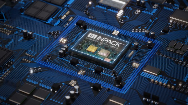
Advanced Packaging
Advanced Packaging is a blanket term used to describe a general grouping of various distinct methodologies. Advanced Packaging technologies include: 2.5D, 3D, Fan-Out (2D), Wafer Level Packaging and System-in-Package (SiP).
About System-in-Package (SiP) Technology
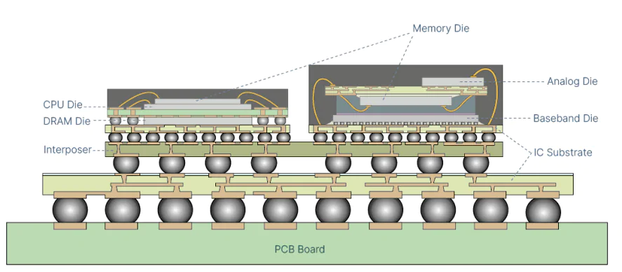
SiP is a combination of multiple active electronic components of diverse functionality, assembled in a single unit, that performs multiple functions associated with a system or sub-system.
SiP may optionally contain passives, MEMS, optical components and other packages or devices; including a combination of bare dies and SMT components.
SiP is designed to be a complete system within a single package, whereas a Multi-Chip-Module (MCM), containing two or more interconnected chips, isn’t necessarily a complete system.
Advanced Packaging Technologies
SiP / MCM Packaging
Heterogenous Integration
3D / 2.5D Packaging


2D Packaging = Integration method of mounting 2 or more dies horizontally on the surface of the substrate:
Takes up less space and provides more functionality compared with SMT
CTE matching, reinforced structure, good thermal dissipation solution
2.5D Packaging = 2 or more active semiconductor chips placed side-by-side on a silicon interposer for extremely high die-to-die interconnect density:
Takes up less space than 2D, when using high IO dies
Improved thermal and CTE matching
Reinforced structure
3D Packaging = Multiple layers/chips/wafers, stacked vertically and electrically interconnected, to enable die-on-die and package-on-package solutions:
Optimizes functionality
Superior system design featuring thermal, CTE and structural advantages


Frequently Asked Questions
What is "advanced packaging"?
“Advanced packaging” is a general term that encompasses several different methods for integrating multiple electronic components. Key technologies under this umbrella include 2.5D, 3D, Fan-Out (2D), Wafer Level Packaging, and System-in-Package (SiP).
What is the fundamental difference between 2D, 2.5D, and 3D packaging?
The primary difference lies in the physical arrangement and interconnection of the semiconductor dies:
- 2D Packaging: Mounts two or more dies horizontally on a substrate’s surface.
- 2.5D Packaging: Places two or more active chips side-by-side on a silicon interposer, enabling very high-density connections between them.
- 3D Packaging: Stacks multiple chips or wafers vertically and connects them electrically for die-on-die or package-on-package solutions.
How does a System-in-Package (SiP) differ from a Multi-Chip-Module (MCM)?
While both integrate multiple chips, a SiP is designed to be a complete functional system or sub-system within a single package. In contrast, an MCM simply contains two or more interconnected chips and does not necessarily constitute a complete system.
What kind of components can be included in a System-in-Package (SiP)?
A SiP is highly versatile and can integrate a wide variety of components. This includes multiple active electronic components, bare die such as Si, GaAs, GaN, SMT components, as well as other elements such as passives, MEMS, and optical components.
What are the main advantages of 3D packaging in system design?
3D packaging offers superior system design advantages by stacking components vertically. This configuration optimizes functionality and provides significant benefits in the final dimensions of the solution as well as better functionality.
What is the primary benefit of 2D packaging over traditional Surface Mount Technology (SMT)?
Compared to traditional SMT, 2D packaging takes up less space while providing more functionality. It also offers enhanced structural reinforcement and better thermal dissipation solution.