Multi-chip Modules & System-in-Package Technologies
Yaniv Maydar
|12th January ,2025
MCM & SiP Technologies - Moving Us Forward On the ‘More than Moore’ Road Map
We’re witnessing a rapid evolution in advanced semiconductor nodes and market growth due to the meteoric rise of AI, Mobile, Autonomous Automotive, IoT, Communications and cloud, Health Tech, and Wearables. The various technologies driving the overall functionality of systems and devices associated with these applications have increased exponentially, impacting factors such as device performance, energy consumption, power dissipation, and space (miniaturization).
Development of the System-on-Chip (SoC), combining digital and analog, MEMS and Photonic Sensors, has led to the small form factors used in smartphones, health monitors, smart homes, and more. Advancements in smaller feature sizes and the resulting billions of transistors per chip translate into increased functionality, enhanced performance, and greater power — but these benefits come at a price. SoCs are hugely complex systems that generate very high NRE costs and involve other budgetary, time, and market constraints. For this reason, it has become clear that alternative technologies are now urgently needed.
The System in Package (SiP) Solution:
The heterogeneous integration of separately manufactured components into a higher level assembly — System-in-Package (SiP), is able to leverage the advanced capabilities of packaging technology by creating a system close to the System-on-Chip (SoC) form factor but with better yield, lower overall cost, higher flexibility and faster time to market. A recent paradigm shift from SoC-centric solutions to SiP-centric solutions has occurred, even for high-volume products.
Multi-chip Modules (MCMs):
Differences between MCM and SiP technology are mainly in their respective scope and functionality. The MCM isn’t necessarily a complete system, whereas a SiP is purpose-built to be a whole system within a single package. SiP integrates multiple ICs, along with supporting passive devices, into a unified package, while the Multi Chip Module (MCM) represents a tightly coupled subsystem or module packaged together. However, an MCM can act as a cohesive unit, even though it may not encompass the entirety of the system’s functionality.
A Closer Look at System-in-Package (SiP):
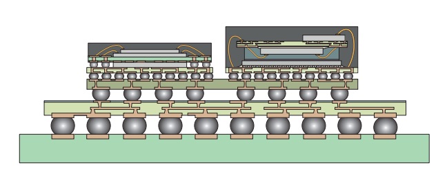
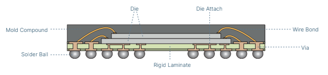
SiP (System-in-Package) Technology is a combination of multiple active electronic components of diverse functionality assembled in a single unit that performs multiple functions associated with a system or sub-system. The SiP may optionally contain passives, MEMS, optical components, and other packages or devices, including a combination of bare dies and SMT components.
SiP typically refers to standard packages (QFN, BGA, CSP, LGA) that can include different semiconductors (Si, SiGe, SiC, GaAs, GaN) and semiconductor technology generations (CMOS 65nm, 45nm, 28nm, 14nm, etc.).
The SiP-tech evolution is focused on an approach based on current and emerging generations of packages and technologies. Currently, more than 1,000 package families, with sub-groups and specialties, are available in the market. Some packages are highly specialized to niche markets, others are customized for specific functionality, while others are still more generic, serving multiple applications.
Successful design concepts will depend largely on selecting the right SiP configuration based on specific needs for each application and the availability of the components, which can then be integrated into a SiP using the appropriate technologies, including interconnect technology, die attach and seal or encapsulation technologies.
Various technologies can be used in SiP design, interconnect technologies (vertical and horizontal), encapsulation technologies (protection and stabilization), and packaging architectures. The number of available technologies for SiP implementation is growing rapidly and includes not only side-by-side integration but is also moving towards 3D, with many different interconnect options.

A Focus on Interconnects:
Vertical Electrical Contacts: Through mold interconnection, film-assisted molding, X-via, wire stands embedded interposers, and dies.
Horizontal Electrical Interconnects: High-density line and space using subtractive, mSAP, and SAP processes.
Interconnect Options:
- Wire bonding, including stacking options, using various wire bonding diameters and materials
- Flip Chip, high resolution and high density interconnects, enabling both Fan-In and Fan-Out technology
- L/S High Density and high-resolution line and space, down to 25um in substrates and 2um in RDL technology
- Encapsulation used to protect the sensitive wire bonds and dies from environmental influences
- 3D (PoP) Package-on-Package technology is based on a through-mold interconnect and use of a lid interconnect to enable dies to Fan Out and interconnect vertically.
- Fan-out panel-level packaging (FOPLP) and fan-out wafer-level packaging (FOWLP) are among the latest packaging trends in microelectronics for higher productivity, lower costs, and higher yields.
- Interposers enable interconnect between low and high-resolution substrates, matching CTE, as well as stiffening of the mechanical structure.
Applications — Perspectives
Most of the requirements and challenges SiP technology has faced throughout its evolution is dictated by the needs of the many diverse applications it serves. SiP, with all its challenges, remains a viable alternative to SoC manufacturing. As long as time-to-market and production costs continue to be key considerations, SiP will thrive and grow in mainstream technology.
Power Functionality: Power semiconductors such as Silicon Carbide (SiC), Gallium-Nitride (GaN), and power systems in a package, are becoming readily available due to innovative packaging power dissipation concepts.
MEMS Functionality: Autonomous vehicles and smart homes are main drivers for sensor modules. However MEMS and Sensor Packaging in general add many challenges to the package design picture, such as stress sensitivity, open access to sensor surfaces, and materials and process compatibility in sensing functionality.
Complex IoT Devices / Edge Computing: The Internet-of-Things (IoT) can be described as a paradigm whereby objects equipped with sensors, actuators, and processors can communicate with each other. IoT devices consist of a processor with an IP stack and RF interface and also require sensing abilities to interact with the ambient environment.
What are the Challenges?
- Wiring density in 2D/3D
- Thermal management
- COTS and bare-die co-assembly and processing
- Multi-domain testing challenges
AI Integration into SiP: Artificial Intelligence (AI) in cloud services running large databases. Companies such as Nvidia, Intel, AMD and Qualcomm are aggressively pushing into this technology.
Applications-Related Challenges:
- Functionality increases due to the growing demand for diverse device functionality. Co-designing becomes more relevant.
- Non-electronics to play a more dominant role in functionality. Co-Design of non-electronic functions; optical, mechanical, cooling and others. Previously implemented by separate stakeholders for large systems, will now be integrated by manufacturers early in the value chain.
- Assembly processes will transform challenges in SiP manufacturing, especially for multi-domain (more than Moore) functionalities, which lies in the assembly process itself. Enabling next-level MCM (multi-chip module) technology.
- Reliability requirements must be adapted seamlessly to application needs. Attention to new or unaddressed reliability challenges for sectors such as automotive, aerospace, and satellite.
In Conclusion, SiP remains the most effective TTM, cost, and functionality technology available today. It’s the main option able to move us forward on the ‘More Than ‘Moore’ road map.
Dedicated to meeting your dynamic project needs, PCB Technologies supports our customers across the board – from initial design to completed assembly. Innovation is in our DNA, and the development of advanced capabilities such as IC packaging and miniaturization micro-processes are a big part of our profile.
Contact us now to discover how much ‘Moore’ you can do – Here