‘Moore’ than a PCB – Breakthrough Solutions
Yaniv Maydar
|25th October ,2023
A challenging new era currently faces the semiconductor and microelectronics industry. It’s all about finding solutions to the almost impossible market demands to reduce both the scale and cost of electronic devices while at the same time expanding functionality and performance levels. It brings to mind Moore’s Law – the exponential relationship between technological advancement and lowered costs that drives rapid innovation and market growth.
In order to fulfill market demands, we’ll need access to technological advances that bridge the gap between CMOS solutions and packaging options, offering improved performance and added functionality at a reduced cost. This may be achieved by integrating supplementary electronic modules into end-products.
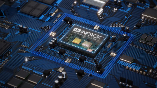
However, solutions are not just limited to reduced costs or CMOS scaling. The real answer may rely on integrating the combined performance potential of many diverse technologies into one innovative high-end PCB — representing a real breakthrough in augmented functionality.
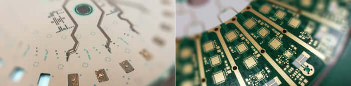
The diversification of technologies could include MEMS Devices / Advanced Sensors / CMOS Image Sensors / Power Electronics / RF Devices and others. This kind of integration can practically eliminate wiring and assembly errors in complex circuit boards while raising automated production levels and reducing labor costs.
But is there ‘Moore’?
- The PCB industry is making remarkable progress; however, market demands are piling up. There’s an urgent need for miniaturization and more efficient interconnect solutions, which is a major factor contributing to the huge market growth of Substrate-like PCB (SLP) solutions.
- Reducing electronic package size is another essential demand towards lowering power consumption and boosting functionality. But because miniaturized components must be placed within extremely limited dimensional constraints, this solution isn’t yet feasible— at least not with conventional printed circuit board technology, but we’re working on it.
- A basic building block in logic devices is the CMOS transistor, which, along with storage components, represents what we term the Digital Content of an integrated circuit. However, many microelectronic products also have non-digital functionalities. Development in both process technology and design is now focused on making CMOS and non-digital technologies more compatible in order to facilitate one super-small, function-packed integrated system.
- Our fast-paced, consumer-driven market is also calling out for advanced System-in-Package (SiP) modules.
Our goal would be to bundle various components like ICs, Passive Components, RF, Modems, etc., into a single package or even onto one PCB. The downscaled component size of a complete system would then be significantly smaller compared with a full set of individual modules, dramatically boosting efficiency and reducing costs.
We offer so much ‘Moore’ than a PCB.
First established in 1981, PCB Technologies rapidly evolved into an industry leader, providing a comprehensive all-in-one solutions approach in the design, fabrication, and assembly of high-reliability, multi-layer, complex boards, unique interconnect solutions, plus ground-breaking miniaturization and advanced IC packaging solutions.
Dedicated to meeting your dynamic market needs, PCB Technologies supports our customers every step of the way – from initial design to completed assembly. Innovation is in our DNA, and the development of near-future capabilities such as proprietary substrates and micro-processes are a big part of our profile.
Contact us now to discover how much ‘Moore’ you can do or learn more about our PCB miniaturization and IC Packaging solutions.