SLP – Substrate-Like PCB Technology

Yaad Eliya
|26th November ,2024
SLP Technology: Next-Generation, High-Density PCB Solution
Outstanding Q&A session about Substrate-like PCBs with PCB Technologies’ CTO Yaad Eliya. Check out the exceptional features and functionality of SLP technology (that fit somewhere between a standard HDI and the micron-scale characteristics of an IC substrate), plus how SLP is influencing the design, fabrication, and PCB manufacturing processes of today’s hottest new products, applications, and near-future innovations.
THE BEST OF BOTH WORLDS:
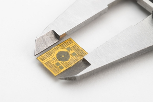
Q1: What exactly is a Substrate Like PCB (SLP)?
A: Experts in the field have asked the question: “Is It a PCB or an IC Substrate?” In a real sense, SLP is a transition from a PCB into a product with package substrate-like features, occupying a middle ground between an HDI PCB and an IC substrates.
Substrate-like PCB design comes into play with the necessity for smaller linewidths; driven by the ever-pressing demand for more compact electronic devices such as smartphones and wearables. Indeed, it’s been the mobile phone giants over the years that have driven PCB vendors to invest heavily in the production of SLP.
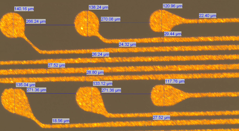
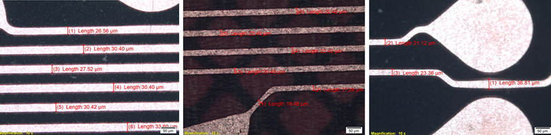
SLP Technology requires line width/line spacing equal to or less than 30/30 µm, which allows reduction in the size of the main board; facilitating more space for additional components. The schematic below shows a progression of Ultra-HDI PCBs and the capabilities required for their fabrication.
| High-Density Interconnect | Substrate-like PCB | IC substrate |
 |
 |
 |
|
|
|
SLP progression of substrate technology
The final point being, that specialist PCB fabricators can introduce SLP technology using a unique family of raw materials with low CTE (=Coefficient of Thermal Expansion@ PPM/C0), enabling a Chip-on-Board (CoB) to be assembled on the substrate alongside regular SMD, press-fit, or wire bonding (AL, Cu or Au wires).
SLP’s can use a subtractive process, a common practice in the PCB industry, and combine it with mSAP (Modified Semi-additive Process) flow.
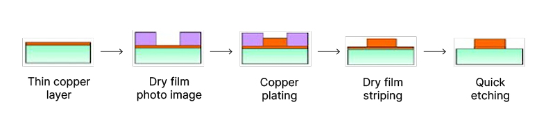
20/25 um L/S, flex, outer layer use of subtractive process not MSAP, SAP
KNOW THE DIFFERENCE:
Q2: How does SLP Technology differ from a traditional PCB or an IC Substrate?
A: SLP is a fast-tracking technology; giving PCB Fabricators the fastest and most direct method of allowing system designers to introduce their system into the market — with guaranteed yields. How does that work you may ask? Mainly because the process by which we build the SLP (dependent upon component type and geometry), already takes into consideration many important factors such as; any mismatch between the die and the substrate, all the assembly steps, temperature ramp up, cleaning and electrical tests, etc. In other words, myriad production details that the designer can’t possibly figure-in beforehand.
Substructive Process Flex – 30/30 um L/S, 30/40 um and 30/50 um L/S for medical application
For example: If the power density (W/mm2) is too high, the heat should be directed elsewhere. Usually, the system engineer utilizes an active dissipation device to extract excessive heat from sensitive components. When we build an SLP with our customers, it gives them access to advanced heat dissipation techniques, such as embedded coins, with low CTE, that pull heat from the component straight into the heat sink, reducing the need for additional active cooling systems (fans, cooling fins or cooling pipes), thus economizing on the extra cost and precious space devoted to these add-on devices. The heat dissipation process is critical step, never the less, it’s not the only important step we are implementing.
The bottom line is, that on a standard PCB you hardly ever design for a Chip-on-Board (CoB) and die cavity, yet with IC Substrates, you hardly ever design for regular SMD components.
WHERE SLP WORKS BEST:
Q3: Which industries / sectors benefit from using SLP Technology?
A: The industries that can benefit from SLP capabilities are practically limitless. It’s already well-rooted in the automotive, aerospace, medical and power sectors worldwide. More recent adopters of SLP solutions are within the communications sector, for servers with HSD (High Speed Digital) data transfer, also for optical systems and for use in semiconductor packaging companies. In the past, aerospace, military and governmental mega-projects were driving the technology, however, in the last 20 years, mobile phone technology has become the clear front-runner in this game.
HIGH EXPECTATIONS:
Q4: Is SLP Technology suitable for high-frequency or high-speed applications?
A: Absolutely yes! Sometimes we even combine RF, Analog and Digital in the same SLP. For external layers, we use low CTE organic substrates with very low/ very high Dk and Df (Dk can go down to 3.0 and up to 9.0) while the Df is comprised of BT epoxy with standard Dk (4.2-4.6) but with low CTE.
Due to the fact that the materials are more homogenous, (finely spread glass fibers, except for M-SAP), it creates straighter, smoother conductive sidewalls that dramatically reduce losses, whereby the remainder of the electrical RF performance can more closely match design simulations.
BRIDGING THE GAP:
Q5: What impact does SLP have on system reliability?
A: When designing a system, from the die through the package down to the PCB, you need to keep a close eye on Coefficient of Thermal Expansion (CTE) mismatch between the PCB and IC substrate. SLP bridges the CTE gap between PCB and IC substrate and die, lowering both costs and production time.
A HEATED DISCUSSION:
Q6: Overheat issues in high power – How can SLP surmount it?
A: Usually by COIN / CMC (Copper Molybdenum Copper) inserts. Thermal management is an ever-increasing issue at the bare PCB and assembly level, especially in high-power and high-voltage applications, where the need for better heat transfer and cooling solutions is critical.
The copper coin heat dissipation method consists of a piece of solid copper inserted onto or into the PCB, typically under the specific component(s) that require cooling. The copper coin provides about X10 the cooling compared to a via farm. Instead of using thermally conductive material, the copper coin can provide direct contact between the heat-generating component pad to the heat sink.
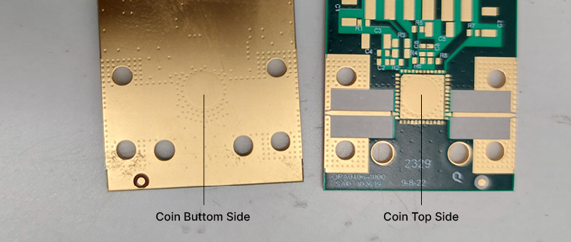
Cu Coin in Hybrid construction/mixed material
Copper coin technology is best suited for a specific or a small number of components on a PCB that are generating the most heat. The copper coin provides the ultimate heat transfer solution in a localized fashion on a PCB regardless of the number of layers or PCB material however, substrate weight is dramatically lower, compared to a heat sink or active cooling elements.
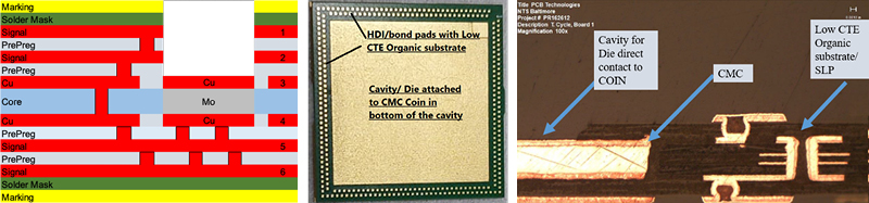
Above: SLP for high power applications and heat dissipation: Buried Coin {Copper Molybdenum Copper} with low CTE, compatible with organic substrate (CTE 5-8 PPM/C)
YOUR BOTTOM LINE:
Q7: Are there cost differences between Substrate-Like PCBs and traditional PCBs?
A: Yes. In the short-term, SLP technology can be more expensive than regular PCBs because of outlay in materials and processes.
In the long run, utilizing SLP is a cost-effective, low-risk option that can actually save money: Because PCB miniaturization isn’t just about saving space; it also reduces power consumption, lowers production costs and cuts time to market. It also allows for easier integration into systems and more convenient part replacements.
SMART DESIGNING:
Q8: Does the design phase for SLP technology require any special considerations?
A: Designers will need to consider the attached die and bonding pads, aside from SMD components, and the distances between them. During the die attach process, SMD components should already be in place.
SLP also has thermal considerations that MUST be taken into account. Due to its close proximity to power-generating components, it is essential to dissipate the heat produced as quickly and efficiently as possible.
WHY YOU GET MORE:
Q9: What added value does PCB Technologies bring to this field?
A: iNPACK (A PCB Technologies Company) is an expert in the field of PCB miniaturization, organic substrates, and enhanced microelectronics. We offer IC packaging technologies with cutting-edge capabilities that deliver comprehensive substrate, panel-level manufacturing, and engineering support to our customers; in fact, they depend on it. Our common design rules (PCB, Substrate & Packaging) are conveniently located all under one roof, providing speedier, high-efficiency services for your peace of mind.

Interested in a competitive edge?
Substrate-like PCB can be counted as a true next-generation PCB, providing a real competitive advantage in the constant race to pack more function into an ever-smaller footprint.
Let’s discuss integrating SLP technology into your projects. Contact PCB Technologies