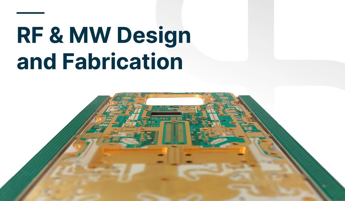
What mSAP Technology Can Do for Your Advanced Applications
Dr. Eran Lipp
|2nd October ,2023
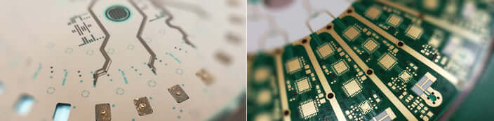
Sharing knowledge is what fuels the PCB industry and that’s precisely why we’re interviewing the man who is taking us Beyond Design Limits at PCB Technologies. R&D Manager of the Circuits Division, Dr. Eran Lipp, answers questions about the many benefits, unique characteristics and varied applications for mSAP (Modified Semi Additive Process) technology.
Q1: Why was mSAP technology developed?
A: mSAP (Modified Semi Additive Process) is a breakthrough workaround that was born out of the necessity to find a quick and more cost-effective alternative to creating high resolution PCBs and substrates.
-
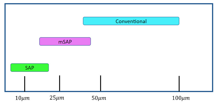
Conventional Subtractive Methods, “print and etch”, enable fine-line definition down to 25um but limit the base Cu thickness to 10um or below; which is incompatible with most applications.
-
SAP (Semi Additive Process) is a more advanced technology allowing resolution down to 5um line/space, but it requires significant changes to be made in standard PCB production lines.
-
mSAP is the midway between the two; allowing high resolution PCBs, down to 25 um line/space with Cu thickness up to 20um, without making any major changes in existing production lines.
Q2: What are the main differences between SAP and mSAP?
A: in both SAP and mSAP, the process begins with a thin base Cu layer, used as a seed for Cu electroplating after resist exposure and development. After electroplating, the resist lines are stripped and a quick etching stage is performed (“flash etch”), which removes the thin Cu seed, thereby isolating the electroplated lines and creating the final Cu image. The main difference between the two methods lies in the thickness and source of the initial Cu layer.
With SAP, the raw material base Cu is fully etched and the seed layer is deposited by sputtering or by an electroless Cu deposition process. Special adhesion layers, such as Ti or W are included in some cases and the resulting seed layer is typically 100-500nm thick. In contrast, with mSAP, the seed is electroplated Cu supplied by raw material vendors in Cu clad laminates, with a typical thickness of 2-5um.
The thin Cu seed used in SAP is removed faster than that of mSAP, resulting in smaller differences between printed and final pattern; thereby allowing higher resolution. The difference in the way SAP and mSAP seed layer is created, not only impacts trace width and resolution, but shape and integrity as well; which in turn affects conductivity, impedance and much of the overall production costs.
Although SAP technology can achieve narrower trace widths and line spacing, your design may not always require those ultra-fine feature sizes. mSAP allows high resolution PCB designs with up to 20um Cu thickness, without the extra cost and complexity of SAP. mSAP offers a significant advantage in that it uses off-the-shelf, quality Cu; easily available at competitive prices. Also, there is no need for sputtering and no adhesion issues.
Q3: When is mSAP your best choice?
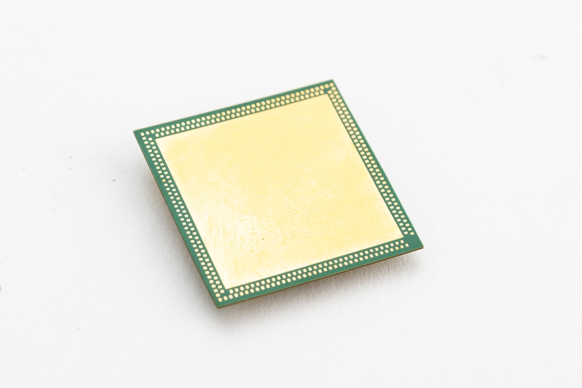
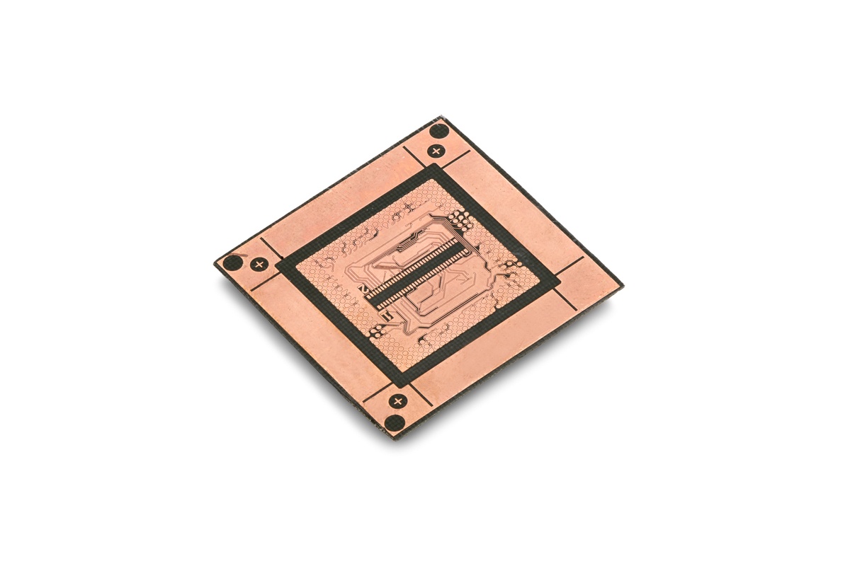
A: Because mSAP technology allows structures in the 20–25-micron line/space range, it’s ideal for high-frequency applications and is commonly used in IC substrate production. It can also offer advantages for interposer PCBs and high-speed PCBs. In addition, any application requiring IC Packaging without the extra cost and complexity of SAP can also benefit from this technology. Such applications include civil and military communications, medical and automotive devices.
Q4: Every technology has its challenges, what about mSAP?
A: There are a few main challenges:
- Controlling Cu seed thickness: Starting with ~3um Cu seed and performing standard dry-film patterning, means all surface preparation steps need to be tightly controlled. An ill-controlled micro-etch process before lamination, may cause surface voids. Lamination parameters should be adjusted for significant change in thermal mass resulting from the thin Cu layer, and resist development may need to be optimized in order to achieve resist features below ~25um line-space.
- Controlling the Cu electroplating process is needed, with uniformities up to ~10% across the board. Cu over-plating results in resist entrapment which interferes with the resist strip and ultimately causes shorts. While underplating results in low conductor Cu thickness, increasing line resistance and aggravating circuit thermal issues.
- Resist removal after electroplating may require non-standard stripping chemistry. Failure to remove the resist results in resist islands or left-over scum; interfering with the flash etch stage, resulting in shorts.
- Controlling the flash etch process: This is the most critical process in mSAP. Over-etching means lower conductor Cu thickness, reduced line width and increased space, while under-etching causes shorts.
Q5: Does mSAP require special manufacturing equipment /Capex?
A: In general, to stay competitive in today’s market of shrinking electronic devices, PCB manufacturers will need to make provisions for upgrading existing machines, and plan for future investments in higher-end equipment.
- Imaging equipment (either direct imaging or laser dot imaging) – with mSAP, printed resist lines become Cu spaces, which are widened in the flash etch process with typical roll-off values of 6-10um. Resist lines as small as 15um should therefore be printed in order to realize 25um line/space in the final Cu image.
- Resist removal equipment should be tailored for mSAP, ensuring an appropriate process window with no risk of unstripped islands or scum.
- The flash-etch stage may require special equipment to allow for a well-controlled process.
Q6: How does PCB Technologies answer demanding customer requirements?
A: Customers depend on us as dedicated partners, from the initial PCB design phase and beyond. Our critical input at the board design stage includes image modifications to enhance product yield and manufacturability, stack-up material selection for optimal electrical and thermal performance, plus thermal and RF simulations.
Our capabilities building complex boards allow us to meet low tolerance requirements, and by utilizing many advanced technologies and processes, like mSAP, we’re able to pass on a wealth of expertise to our customers; fulfilling their needs for quality customized solutions.
PCB Technologies is so much more than a board manufacturer and supplier. Our All-in-One capabilities span the entire process, from prototype to mass production for industries such as Aerospace, Military & Defense, Medical and many others.