About iNPACK
We go beyond design limits to offer you cutting edge semiconductor and electronics assembly, testing and IC package design including LGA, BGA and 2D & 3D customized solutions. Featuring fully supported automated processes, MW microelectronics assemblies, System-in-Package (SiP) & heterogeneous integration. We also offer high level expertise in organic substrate design and manufacturing based on advanced materials, subtractive and mSAP processes.
Miniaturization Technology
- IC Packaging & System-in-Package (SiP) design
- Semiconductor assemblies
- MW microelectronic assemblies
- Organic substrates
- Process development & DFM processes
iNPACK Benefits
- Time To Market (TTM)
- Design & manufacturing under one roof
- Cost effective solutions
- Innovative approach
- Customization options
- In-house capabilities: substrates, PCB, micro assembly

AS9100

ISO 13485

ITAR registered

RMI

ROHS

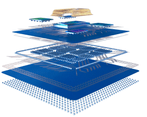
Advanced IC Packaging & Organic Substrates – All-in-One Solutions
We offer organic substrate expertise with high-density line/space width and advanced packaging that allows for a smaller form factor, increased functionality, high thermal conductivity, and improved process stability. System-in-Package (SiP) prototypes, or low/mid volume production, Multi-Chip-Modules (MCM), and more; all compatible with aerospace, defense, medical, and other top industry needs. We specialize in heat dissipation solutions that ensure your projects meet high standards of performance and reliability in the shortest possible time to market.
Organic Substrates
Advanced Packaging Assembly
Our unique assembly process designs enable you to achieve high-level, customized results with IC packaging solutions tailor-made to your specific applications. Our customers are no longer bound by a specific design process dictated by individual fabricators or semiconductor packaging companies. Instead, we offer you the design freedom to choose from a variety of custom options perfectly aligned with your project needs: Antenna-in-Package, Flip-Chip, QFN package technology, Filter-on-Package, and many more.
Advanced Packaging
Technological Edge
iNPACK are experts in organic substrates and enhanced micro-electronics packaging technologies, with cutting-edge capabilities that deliver complete, comprehensive substrate panel-level manufacturing and engineering support to our customers; in fact, they depend on it. We continuously work to improve interconnections between PCB, Substrate and Semiconductors through advanced technological know-how. Solutions include Organic Substrate materials, IC Substrates, Die Packaging, Multi-Chip-Module (MCM) technology, Chip Packaging and more. Creative solutions and enhanced design flexibility give us the ability to deliver high-speed, thermal and RF pathways that simplify integration processes, that improve overall system reliability. Our common design rules (PCB, Substrate & Packaging) are conveniently located under one roof; providing speedier, high-efficiency services, for your peace of mind.
Organic SubstrateRelevant Services
SiP Design
Advanced System-in-Package (SiP) solutions are multi-component, multifunction products that leverage PCB Technologies’ core strengths in order to offer our customers higher levels of miniaturized integration with reduced lead times. These include:
- Packaging solutions
- Size reduction
- High thermal conductivity
- Ultra-thin with fine lines & spacing
- Controlled CTE
- 3D design
- Shielding options
- Sealing solutions
- Fine pitch flip-chip and copper pillar
- Double side assembly
- Development & production testing
- Turnkey solutions
We offer a high-efficiency All-in-One Solution, resulting in brighter ideas and better-quality products at significantly shorter lead times. Our advanced R&D center, located within the same large complex as our manufacturing facilities, allows for the seamless creation of custom SiP; from design to manufacture, assembly, and testing.
Purchasing
The PCB Technologies procurement department acquires raw materials from our trusted global network of suppliers located in Asia, Europe, and North America. Over decades, we’ve built up a robust supply chain of strategic partnerships that consistently provide us with proven quality, reliable service, and cost-effective solutions.
DfX/DfM
An entire suite of Design for Manufacturing (DfM) services that expertly analyze PCB designs with the aim of improving quality, yields, and delivery times while also reducing costs.
- Careful evaluation identifies potential setbacks early in the PCB design stage, where we waste no time in recommending alternative methods to help boost quality, lower costs, and speed up TTM.
- Our DfM engineering analysis examines the PCB production process layer by layer, checking out all available options, such as reducing the number of layers or consolidating components in order to cut costs sensibly and responsibly.
- By conducting post-build reviews after every production cycle, we reveal additional methods of streamlining manufacturing for better yields at lower costs.
Design for Testability (DfT) services help to identify possible snags with PCB designs before starting mass production, minimizing defects while maximizing reliability and repeatability.
The In-Circuit Test (ICT) can pinpoint defects in the board from the assembly process, such as component mismatches, misplacements, or missing components. PCB Technologies also delivers functionality tests, whereby PCBs are tested in their final production environment to ensure proper functionality according to specs.
Our Value Analysis/Value Engineering (VA/VE) solutions enable customers to gain the maximum value from their PCB designs. Unlocking greater product value through continuous improvements is facilitated by combining our services: Design for Manufacturing (DfM), Design for Testability (DfT), Design for Procurement (DfP), Design for Cost (DfC), and Design for Assembly (DfA).
PCB Technologies works hand-in-hand with customers not only to improve existing PCB designs but also to support clients’ new product designs, from launch through scaling-up production and long-term management.
Circuit Editing
PCB Technologies supports PCB designs at all complexity levels. Our expert teams are available to advise customers on optimal PCB materials, structures, and designs best suited to their unique product needs.
This includes optimization of component placement, EMC optimization and impedance checking, thermal management, DfM, high-speed, and more. We also design PCBs to meet specific standards, such as HDMI, MIPI, LVDS, PCIe, DDR3, LPDDR3, and DDR4.
Comprehensive Testing Plan
Testing is a crucial part of the PCB Design & Assembly Process. We work closely with our clients to identify the optimum testing requirements for each unique project.
Our cutting-edge in-house testing capabilities enable us to carry out the most comprehensive and highly efficient test procedures across the entire production process and through to final inspection. Our customers can be confident that every PCB meets the same high-quality standards from start to finish.
Reballing & BGA Replacement
Well-equipped to perform various kinds of rework operations on both electronic and mechanical assemblies, per customers’ requirements, PCB Technologies offers BGA and QFN components rework using a dedicated state-of-the-art ERSA rework machine, with the latest technology in Infrared BGA Re-balling.
NPI - New Product Introduction
We have extensive experience providing a range of New Product Introduction (NPI) services. Our primary operational model allows for speedy delivery, with full management of NPI activities that encompass supply chain management, technical overview, and engineering overview.
Our clients enjoy a seamless product transition from prototype to production that includes the design and fabrication of dedicated tooling.
Bare Die & Component Sourcing
PCBs are only as good as their constituent components; that’s why sourcing is such a critical operation. Over the years, PCB Technologies has grown a strong, stable global network of strategic partners, providing us with the purchasing power to source the very best components at comfortable prices.
We source the most compatible components for any and all customer requirements, helping to optimize costs by managing set-up and storage. Our experts will suggest alternative components, when necessary, to ensure a secure line of supply.
Full Turnkey
With a long history of cutting-edge PCB design expertise, coupled with top-tier production capabilities, our customers rely exclusively on PCB Technologies for their PCB Full Turnkey projects.
We utilize the latest technologies and automation equipment to create high-quality production processes; tailored to the product requirements. Solutions involve all aspects of assembly — efficiently transforming part integration, cabling, and electronics, into modules or end products. Customers also benefit from our broad market purchasing power in sourcing the best components at cost-effective prices.
Shipping
Full System Integration
As a One-Stop-Shop solutions provider, PCB Technologies adopts an all-in-one approach in the design, fabrication, and assembly of high-reliability, multi-layer, complex boards, unique interconnect solutions, plus ground-breaking miniaturization and advanced packaging solutions, all under one expansive roof.
Our comprehensive range of services includes advanced PCB design, manufacturing, assembly, box-building and testing, thermal management, High Current, High Frequency, High Speed, HDI, Sequential Lamination, Rigid, Flex, Rigid-flex materials, and much more.
An on-site, certified cleanroom manufacturing facility ensures that sensitive PCB components are free from contamination. We have the following certifications: ISO9001/ISO14001/ISO13485/TSI16949) and are compliant with ESD requirements. The results are higher quality and better lead times.
Planning

Talk to an Expert
Frequently Asked Questions
What line/space density can iNPACK achieve in their organic substrates?
iNPACK supports 25 µm line/25 µm space, ideal for SiP and HDI PCB applications where fine-pitch signal routing is critical.
What packaging formats are supported?
Offerings include LGA, BGA, flip-chip, antenna-in-package, and advanced filter-on-package, covering both 2D and 3D packaging needs.
How does iNPACK manage thermal challenges?
iNPACK embed CuMoCu “coins” in organic substrates for enhanced heat dissipation and structural stability, doubling electronic functionality in tight form factors.
What is the typical TTM (time-to-market) for SiP projects from design to prototypes?
iNPACK offers quick-turn SiP fabrication as well as a wide range of IC packaging design capabilities in as fast as 6 -8 months, including ramp to mid-volume production.
Are quality certifications in place?
Yes—AS9100, ISO 13485, ITAR-registered, RoHS, and RMI-compliant—enabling automotive, aerospace, and medical-grade assurance.
What testing capabilities are offered in-house
Testing includes design-for-testability (DfT), in-circuit test (ICT), functional testing, and customized ATE testers.
What heterogeneous integration technologies does iNPACK support?
iNPACK offers 2.5D/3D MCM, heterogeneous die stacking, and embedded passives and active components, enabling compact Multisubstrate modules.
How does iNPACK ensure signal integrity for RF components?
By embedding optimized RF pathways, minimizing parasitic inductance, and adhering to controlled impedance designs through substrate/platform consistency.
What is the thinnest HDI substrate achieved?
We work with laminates and prepregs with thicknesses as low as 60 µm, enabling ultra-thin form factor designs.
How is component embedding utilized?
We embed active and passive components directly into the PCB/substrate stack-up to minimize external SMT count and support higher integration density.
What turnkey capability ensures form factor minimization?
With iNPACK capabilities, we integrate PCBs, substrates, packaging assembly, thermal solutions, and testing under one roof—cutting BOM count and optimizing miniaturization.
iNPACK Relevant content
See All Articles
articles
Multi-chip Modules & System-in-Package Technologies
articles
iNPACK™ Panel Level Solutions
PCB Technologies’ iNPACK Division offers complete package PCB assembly solutions for both low and high-volume requirements. This includes SiP-system in package design and manufacturing, surface mount tech, chip on board (COB), microfabrication, and substrate design and manufacturing capabilities.
articles