Focusing on Substrate PCB Manufacturing
Yaniv Maydar
|8th June ,2025
Introduction:
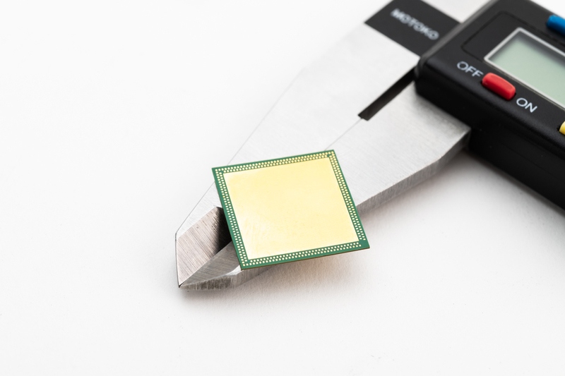
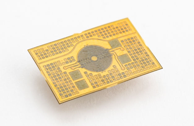
Simply put, substrates PCB are the core support material for IC packaging. They function as a mechanical structure, as well as an electrical interconnect for one or more devices, providing heat management and even acting as passive components. Substrates are used to fan out the die, semiconductor, and fine pad pitch to a coarser pad pitch and, most importantly, to provide a pathway for the device to communicate with the rest of the system.
Critical components in the semiconductors packaging industry, substrates have a first-order effect on device performance, influencing signal integrity, heat management, mechanical structure, and life-time reliability, as well as total package (product) cost. In fact, more than 40% of the entire package cost is attributed to the substrate.
Substrates are custom-designed based on a unique device bond pad, bump pattern, or often on a predefined BGA ball pattern. Substrate design may take weeks or months, followed by a challenging PCB manufacturing process that, on average, takes between 6 to 12 weeks. If performance levels after testing are found to be insufficient, an additional cycle may be required.
PCB substrate material selection and design are some of the most critical aspects of packaging. Substrate type and cross-section (stack-up) are highly dependent upon the following factors:
-
- Bump Pitch
- Line & Space
- Electrical Requirements / Signal Integrity
- Required Stack-Up / Final Thickness
Depending upon device requirements, substrates can be architected and designed for wire bond or flip chip dies.
PCB Substrate Types:
The most commonly used substrates are the ceramic and organic types. Advanced substrates to support finer bump pitch can be made of glass, silicon, various silicon compounds, thin films, etc. However, the vast majority of substrates in the market are organic-based; supporting a device bump pitch of greater than 150 um and trace width/spacing of greater than 20 um, whereas a silicon interposer is widely used to fan-out devices with a finer bump pitch; typically less than 100 um and finer trace width/spacing, typically less than 10 um.
Rigid or Flex: Among the variety of substrates available, major categories are; organic-based rigid substrates and flex substrates. Substrates are classified in terms of mechanical strength. Rigid substrates are mechanically rigid and thicker, while flex substrates are flexible and thinner.
-
- Flex substrates are made of high strength and temperature polymeric materials such as polyimide.
- Rigid substrates can be made from ceramic or organic materials (organic small molecules or polymers).
Organic Substrates: Today, organic substrates have overtaken the ceramics market due to their finer line and space capabilities, better heat management solutions and their ability to add flexibility to the design. Organic rigid substrates are classified into two categories: Laminate and Build-Up Types.
Laminate Substrates: Considered a low-cost substrate in the industry, laminate substrates are widely used in wire-bonded BGA packages to produce low-cost packages. They are constructed by stacking layers of thin laminate materials with double-sided copper foil. Common laminate materials are FR4 which is epoxy-based, and Bismaleimide-Triazine (BT), a higher performance, more advanced resin-based material. For packaging applications, BT is the preferred option and has become standard for BGA substrates.
Laminate substrates can have several stacked layers (2, 4, 6 or more). Connection between layers is in a vertical direction and is achieved using vias. Various types of vias are used to connect layers and to route and transition signals among the layers.
Vias can be broadly categorized as: micro, blind, buried, and through-hole types.
-
- Through-hole via: Goes through the entire PCB from the top layer to the bottom layer. …
- Blind via: Connects an outer layer of the PCB to an inner layer, but does not go through the entire board. …
- Buried via: Buried completely within the PCB layers and does not connect to a surface layer.
- Micro-via: Drilled by lasers having a smaller diameter compared to standard through-hole vias.
Build-Up Substrates: These types of substrates are constructed by sequentially adding thin, non-reinforced epoxy layers (build-up layers) on both sides of a thick laminate core. A thick core is used for mechanical support and as a base to add the build-up layers on both sides symmetrically. A build-up substrate is defined by a core and number of build-up layers.
-
- For example, a 4-layer build-up substrate is denoted as 1 + 2 + 1 or 1/2/1, where 1 means one build-up layer and 2 means a laminate core with 2 metal layers, one metal layer on the top and one metal layer on the bottom of the laminate core.
- Core thicknesses vary from 200 to 1200 um. The industry standard thickness is 800 um. 400 um or less are typically used to address signal/power integrity requirements. The main function of core thickness is for mechanical stability and strength, in order to prevent warpage during assembly and package qualification.
Meeting Your Requirements:
At PCB Technologies, our expertise extends beyond manufacturing to encompass the full spectrum of system-aware substrate design. We specialize in organic substrate development tailored not only for optimal electrical and thermal performance, but also to meet broader system-level needs such as mechanical integration, miniaturization, and reliability. This is part of our heterogeneous engineering approach, where electrical, mechanical, and thermal domains are co-optimized from the earliest stages of design. By combining deep materials knowledge with advanced simulation and design-for-manufacturing principles, PCB Technologies delivers substrate solutions that are custom-engineered to support next-generation IC packaging challenges—today and into the future. We invite you to consult with one of our trusted experts today.