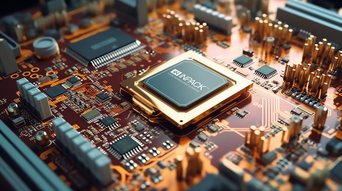
iNPACK™ Panel Level Solutions
Yaniv Meydar
|5th February ,2024
Introduction
The Panel Process, or ‘Panelization’, involves producing a single large board consisting of multiple smaller boards that, once assembled, can then be broken up or depanelized back into individual PCBs. This production method helps improve manufacturing proficiency by minimizing assembly defects and reducing production costs. It’s popularly used for smaller or odd-shaped PCBs.
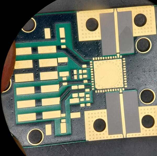
Advanced design and manufacturing capabilities covered by PCB Technologies’ iNPACK Division include System-in-Package (SiP), Surface-Mount Technology (SMT), Chip-on-Board (CoB), Microfabrication, Substrate solutions, and much more.
There are many advantages to using Panel Solutions:
- High Volume Production: Need a lot of boards? ‘Panelization’ saves time and money.
- Product Safety: ‘Panelization’ can reduce shock or vibration during PCB assembly.
- Speed & Efficiency: ‘Panelization’ makes production processes and testing faster and more efficient.
- Better Design: Designing with ‘Panelization’ in mind helps prevent production delays and costly redesigns.
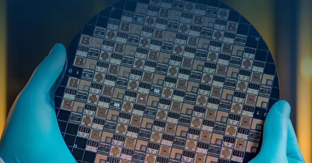
iNPACK FAB was designed with the option to run panels of 100×200 mm2. This technology enables the design and production of large packaging solutions, system level solutions and efficient standard packaging solutions. Both standard packages and customized processes are on offer, by combining iNPACK capabilities with the vast industry expertise built-in to PCB Technologies, its parent company.
Our customers enjoy a truly unique added-value proposition utilizing an exceptional packaging process that incorporates:
- Advanced Substrates
- SMT & Micro Assemblies
- Molding and Through-Mold Interconnect Options
- Air Cavity 3D Interconnect Solutions
PCB panel designs hugely impact the success or failure of individual components and the overall cost of a project.
Why chose iNPACK?
- To provide customers with high-end technology that improves signal integrity and reduces unwanted inductance, PCB Technologies established its subsidiary company iNPACK; experts in system-in-package (SiP) solutions.
- Standard & customized substrate solutions for specific use cases and needs. Combining iNPACK’s subtractive and M-SAP processes with PCB Technologies’ extensive materials knowledge, helps us solve common challenges such as coefficient of thermal expansion (CTE) mismatches, thermal management issues, and more.
- iNPACK makes a global impact providing SiP, semiconductor packaging, organic substrates (25µm lines and 25µm spacing), and 3-D, 2.5-D and 2-D packaging solutions for aerospace, defense, medical, consumer electronics, automotive, energy and communications industries worldwide.
- iNPACK incorporates innovative interconnects as part of its substrates and micro-assembly process capabilities. These technological solutions can more than double the electronic functionality in the same form factor and create substrate-like PCBs.
- Customer support as it should be. We’re always available to discuss your project needs from initial concept to completed assemblies, with quick turnaround times you can rely on. Our goal is to fully support customers through every stage of the process; design, production and beyond, all under one roof, while utilizing unified design rules.
Let iNPACK ensure the success of your next project.
Contact us to find out about more innovative processes that can be implemented on a panel level.