Die Stacking Technology Where Less is Moore in PCB Design & Manufacturing
Yaniv Maydar
|15th July ,2025
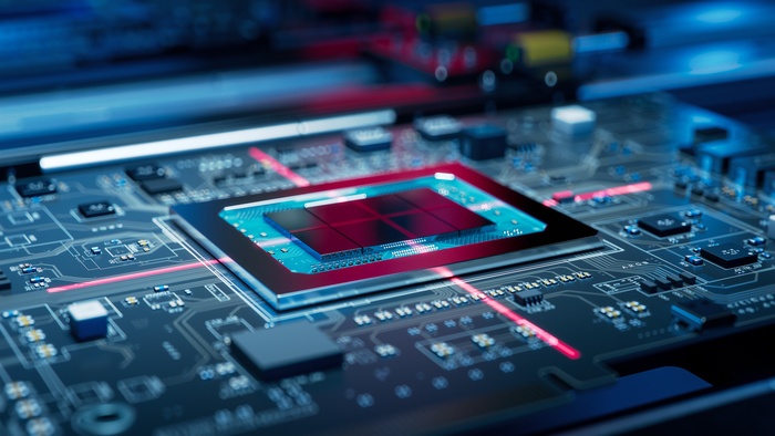
Die Stacking technology involves multiple dies stacked on top of one another to interconnect vertically by means of through-silicon vias (TSVs). Major benefits of the Die Stacking approach are manifest in improving advanced electronic device performance and functionality. Such improvements can include shorter interconnect wire lengths to boost performance while lowering power consumption or smaller form factors that allow for higher packaging densities in a smaller footprint.
Various Die Stacking options exist; however, common methods include the use of a Silicon Interposer (a thin piece of silicon to connect the dies). Dies can be bonded to the interposer by solder bonding, adhesive bonding, or stud bonding. Another common Die Stacking method is the Flip-chip Assembly, whereby dies are bonded directly to the PCB pads. It presents a more complex process than the Silicon Interposer but provides superior electrical performance.
See also: PCB Manufacturing Processes
Main Advantages of Die Stacking:
Space-saving is a key benefit of Die Stacking that impacts almost every aspect of device performance and functionality.
Signal Integrity: By placing closely connected components vertically, Die Stacking minimizes signal distance, allowing for improved signal integrity. This results in faster signal transmission, reduced crosstalk , and lower power consumption.
Thermal Solutions: Die Stacking generates more usable surface area on the substrate, so there’s more space available for other components, such as heat dissipation solutions like heat sinks. This can significantly boost reliability, especially in high-power applications.
More Functionality: Die Stacking allows more functionality in a far smaller space. The resulting higher integration density supports miniaturized PCBs in specialized devices and applications, where a substantial reduction in size and weight are critical factors.
Smaller Form Factor: By stacking components vertically, PCBs can be made thinner and significantly more compact. This enables the design and manufacture of smaller, lighter devices, ideal for portable electronics, wearables, and other space-conscious applications.
Reduced Layer Count: Die Stacking can help eliminate the need for additional PCB layers, which in turn simplifies fabrication processes and potentially lowers costs. It also creates more critical routing space on the existing layers for additional components.

Main Challenges in Die Stacking:
Thermal Management: Each die generates its own heat, so imagine the output of an entire stack. Adequate heat dissipation is a must for Die Stacking designs: heat sinks, interposers, cooling systems, and access to new and innovative heat management techniques.
Mechanical Stability: Every successive layer in a die stack adds additional weight and possible stress. Utilizing innovative materials, such as flexible interposers and special bonding methods, can go a long way in protecting the stack from excessive weight or vibrations. Limited repairability in a stacked configuration is also a challenge.
Signal Integrity & Efficiency: Multi-layered circuitry demands perfect precision and low resistance to dispel signal degradation or crosstalk. These solutions require a deep understanding of advanced package design and routing techniques.
What truly sets iNPACK apart in the OSAT landscape is our vertically integrated, heterogeneous engineering model — bringing PCB, substrate, and full system-level capabilities together under one roof. This in-house synergy allows us to design, simulate, and manufacture tightly aligned solutions that address not just component performance, but also thermal dynamics, signal integrity, and mechanical reliability — all in the context of the complete system. Whether you’re pursuing ultra-miniaturization, 3D integration, or advanced packaging for high-performance applications, iNPACK delivers a seamless path from concept to volume — with precision, flexibility, and speed.
Get started with your next project, knowing iNPACK’s design and fabrication experts are on your side. Give us a call anytime to find out how we can work together.