An In-depth Look at Wire Bonding Options
Yaniv Maydar
|26th November ,2024
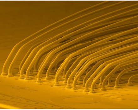
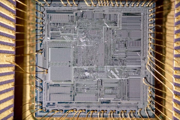
Wire bonding is a common fabrication process used in semiconductor packaging to create electrical connections between a semiconductor device (such as a chip or die) and the packaging substrate, enabling signal transmission, power distribution, thermal management, and more within the device. The proper selection of wire bonding techniques, wire materials, bonding parameters, and process controls will result in optimal wire bonding connections for a wide range of applications.
Wire Bonding Techniques
The two main types of wire bonding techniques are Ball Bonding and Wedge Bonding. Selection of these techniques and variations should be based on the type of application, design requirements, IC packaging technology, and material compatibility. Each wire bonding method presents its own unique advantages and limitations; therefore, choosing one over the other will be dependent upon the specific needs of the semiconductor device and overall packaging strategy.
Ball Bonding:
- Thermo-sonic Ball Bonding (TSBB): A widely-used ball bonding technique involving ultrasonic energy and heat to create a metallurgical bond between a small metal ball (typically gold or aluminum), and the bonding pads on the semiconductor device and the substrate. The ultrasonic energy causes the ball to deform, bonding to the pads.
- Ultrasonic Ball Bonding (UBB): Similar to TSBB, this technique uses ultrasonic energy to create the bond. With UBB, the bonding occurs at room temperature without additional heat.
- Impact Ball Bonding (IBB): With this technique, the ball is formed by the impact of a wire on the bonding pad. The impact creates deformation and forms a bond.
Wedge Bonding:
- Thermocompression Bonding (TCB): The technique uses heat and pressure to create a bond between a thin wire (typically aluminum or gold) and the bonding pads. As heat softens the wire, pressure is applied to form the bond.
- Ultrasonic Wedge Bonding (UWB): Ultrasonic energy is used in conjunction with pressure to create a bond between the wire and the bonding pads. This method is similar to thermos-sonic ball bonding but uses a wedge tool instead of a ball.
- Non-Ultrasonic Wedge Bonding: In this variation, wedge bonding is created without the use of ultrasonic energy.
Fine Pitch Bonding:
- Fine Pitch Ball Bonding: Used for applications with very small pad pitch requirements. It involves ball bonding with smaller ball sizes and finer wire diameters.
- Fine Pitch Wedge Bonding: Similar to fine pitch ball bonding, although it is adapted for applications with tight pitch requirements using wedge bonding.
Reverse Bonding:
- Reverse Bonding (Stud Bumping): With this method, the wire is bonded to a stud bump on the substrate instead of bonding to the chip. It is a technique often used in flip-chip packaging.
Wire Bonding Materials & Diameter Selection
Selecting the most suitable wire bonding materials and diameter is crucial to the semiconductor packaging process. This decision, however, can be influenced by various factors such as electrical and thermal requirements, reliability issues, and cost.
Wire Material Selection
|
Wire Material |
Advantages |
Considerations |
|
Aluminum (Al) |
|
|
|
Gold (Au) |
|
|
|
Copper (Cu) |
|
|
|
Silver (Ag) |
|
|
|
Palladium-coated Copper (PdCu) |
|
|

Wire Diameter Selection
- Thermal Considerations: Larger wire diameters generally have higher thermal conductivity and are used in applications where heat dissipation is an issue.
- Electrical Requirements: Smaller wire diameters can create an advantage in applications with tight pitch requirements and high-density interconnections.
- Mechanical Strength: Thicker wires can increase mechanical strength; an important factor in applications with high mechanical stress or thermal cycling.
- Wire Bonding Equipment Compatibility: It is important to ensure that the chosen wire diameter is compatible with the capabilities of the wire bonding equipment being used.
- Application-specific Issues: In certain applications, electrical and mechanical requirements should be taken into consideration, as in the use of smaller diameter wires for selected high-frequency applications.
- Wire Bonding Yield: The thinner the wires, the more challenging they may be to bond, potentially affecting yield. Consider the capability of the wire bonding equipment and the requirements of the application.
Bonding Process
First & Second Bond: The strength of both first and second bonds is often influenced by factors such as bonding materials, bonding parameters, and the specific wire bonding techniques being used. Generally, the first bond is the stronger of the two:
- First Bond: Whether using a ball bond or wedge bond, the first bond will typically undergo a more controlled and optimized bonding process. During the first bond, the wire is attached to the bonding pad on the semiconductor device or substrate; forming a metallurgical bond is critical for establishing the initial electrical and mechanical connection.
- Second Bond: In processes with sequential bonding (such as a ball in ball bonding), the second bond is formed on top of the first bond. Although designed to be strong and reliable, the second may not have the same level of energy input and process control as the first. The looped wire from the first bond may also introduce additional complexities, requiring process conditions to be adjusted accordingly.
Bond Strength
The strength of the bonds is key to ensuring the overall reliability of the wire-bonded semiconductor device. Manufacturers carefully optimize the bonding process parameters to achieve bonds with the desired electrical and mechanical properties. Both first and second bonds must meet specific industry standards and reliability requirements to ensure the long-term functionality of the device.
- Energy Input: The first bond usually receives a higher level of energy input during the bonding process, contributing to the formation of a strong metallurgical bond.
- Controlled Conditions: The first bond is often formed under more controlled conditions, optimizing parameters such as ultrasonic energy, bonding force, and temperature to achieve the desired bond strength.
- Wire Deformation: The first bond involves a direct attachment of the wire to the bonding pad, allowing for controlled wire deformation. In the case of sequential bonds, the looped wire from the first bond may create additional issues for consideration.
- Bonding Parameters: These may need to be adjusted for the second bond, with the looped wire undergoing a different deformation process. Although efforts are made to ensure a strong second bond, it may not always match the strength of the first.
Additional Factors to Consider:
- Comprehensive Analysis: Before selecting wire bonding materials and diameter, carefully research the specific requirements and constraints of the application, along with costing, reliability, and manufacturability. Consult with wire bonding suppliers and manufacturers for feedback relating to the methods, materials and processes best suited to the application at hand.
- Environmental Conditions: The operating environment can have a direct impact on the long-term reliability of the wire bonds. Environmental factors to consider include; temperature, humidity and potential exposure to corrosive substances.
Test, Validation & Standards: Performing the required testing and validation procedures ensures that the chosen wire bonding material and diameter meet specifications and reliability standards. Adhere to industry standards and recommendations for wire bonding materials and diameters relevant to the application.
Material Plating Processes
Wire bonding materials often require compatible plating systems to help enhance performance and reliability. Plating serves as a protective layer to the bonding pads, preventing oxidation and promoting stronger metallurgical bonds during the wire bonding process.
|
Wire Material |
Advantages |
Considerations |
|
Aluminum (Al) |
|
|
|
Gold (Au) |
|
|
|
Copper (Cu) |
|
|
|
Silver (Ag) |
|
|
|
Palladium-coated Copper (PdCu) |
|
|
Plating Pointers
Make sure industry standards and guidelines are met when selecting compatible plating systems for wire bonding materials. Performing test and validation procedures will safeguard performance and reliability levels for the specified application.
- Surface Finish: The choice of plating systems is often associated with the surface finish of the bonding pads. Refer to common surface finishes shown in the table above.
- Wire Bonding Equipment Compatibility: Ensure that the selected plating system is compatible with the wire bonding equipment being used in the PCB manufacturing process.
- Application-specific Requirements: Pay attention to the specific requirements of the application, such as environmental and thermal considerations, in addition to long-term reliability.
In Conclusion — Wire Bonding Today
Wire bonding technology has evolved over time to keep up with the demands of today’s smaller architectures, growing chip complexity, increasing density of interconnects and materials that can stand up to harsh environments.
Interested in talking to wire bonding specialists?
iNPACK (A PCB Technologies Company) for PCB miniaturization, high-density IC packaging, improved electrical performance and so much more.
Get in touch anytime to discuss your next project.
PCB Technologies is a global front-runner in cutting-edge PCB fabrication processes across the board; offering comprehensive in-house capabilities for everything from quick turn-around of new product prototypes, to cost-effective mid to high-volume production. Serving Military/Defense, Aerospace, Medical, RF/Microwave, Robotics, Automation and more.