SiP Reliability Analysis & Testing
Yaniv Maydar
|7th January ,2024
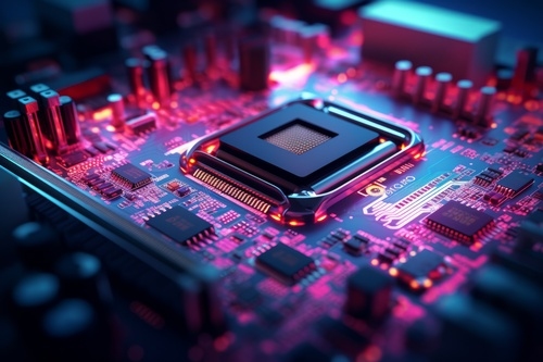
While significant performance, functionality, and form factor improvements are enabled using advanced System-in-Package (SiP) and substrate technologies, it is imperative that a systematic approach and methodology is in place to mitigate thermo-mechanical risk and other challenges associated with SiP solutions.
All designed package structures must be analyzed for reliability in order to have any application value at all. SiP reliability refers to the statistical probability of product failure during its lifetime, stemming from environmental effects, such as temperature, humidity, and radiation, or from the application itself, such as with vibration, pressure, acceleration, etc.
While performing failure analysis for package dependability, possible issues can include warpage, chip cracking, delamination, toughness fracture, plastic deformation, and many other complications besides. Breaking it down further may actually encompass hundreds of failure items, wherein the entire analysis process becomes particularly laborious, requiring more time, higher costs, and additional testing.
To keep it simple, the root causes of dependability issues can be divided into three main categories: Thermal Management, Mechanical Stress, and Electrical Properties.
Although there are many potential failure modes in system design, reliability issues mainly revolve around the following failures: stress fracture, high-temperature deformation, high-temperature deterioration, open circuit, short circuit, line impedance mismatch, electromagnetic interference, and others.
The analysis and testing of temperature, mechanical stress, and electrical system-level reliability issues are summarized in the three sections below. It’s important to note that the implementation of new processes and structures can also introduce new and previously untested reliability issues. If these issues are not detected and resolved in time, they can lead to system abnormalities, causing equipment failure or even major accidents.
Thermal Management
Since no electronic device can operate at 100% conversion efficiency, as some amount of electrical energy is always lost to heat, with its unique advantages of small size and high density, SiP technology helps to achieve system integration. However, due to the dense placement of multiple chips, heat density inside the SiP is higher than that of discrete devices, with heat transfer paths further restricted by the limited space. According to the heat transfer equation, elevated temperatures caused by the SiP configuration is more pronounced than that of packages such as QFN or BGA.
Q = kA∆T/∆x, where Q, k, and A, are heat, the heat transfer coefficient, and the heat transfer area, respectively. ∆T and ∆x represent changes in temperature and distance, respectively. Heat dissipation of the entire system will be impacted, resulting in elevated internal temperatures, if the thermal conductivity issues of the encapsulated system are not resolved.
Irregularities in Mechanical stress become evident in cases of excessive differences in coefficient of thermal expansion (CTEs) of adjacent materials. As the temperature rises due to ongoing heat buildup, component performance is also impacted, which in turn, affects the overall electrical properties of the system. As a result, the majority of reliability issues are actually caused by temperature issues, which necessitate thermal simulation analysis.
Mechanical Stress
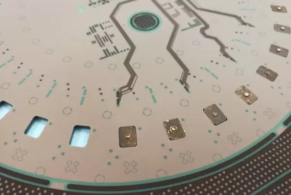
Another important factor in determining the dependability of SiPs is the examination of mechanical stress. In system-level packages, the materials used for the chips, substrates, leads, and solder connections vary. When subjected to influences such as temperature changes or other external environmental issues, various materials will shrink or expand at different rates in accordance with their own unique qualities and structure. This can lead to specific consequences in deformation and mechanical stress.
To illustrate, the formula for CTE: α = ∆l / (l × ∆T)
Where α, l, and ∆l, are the CTE, length, and length change, respectively.
When two different materials heat up, their CTEs vary, creating a noticeably inconsistent strain on system components and resulting in extreme stress conditions. This falls under the category of Mechanical Stress. Loss Failure and Overstress Failure are the two primary types of failure brought on by Mechanical Stress. The former refers to the buildup of low stress continuously applied over an extended period of time, leading to component loss (dysfunction) that produces system failure. The latter refers to failure brought on by an acute stress event or moment that far exceeds the components’ stress tolerance levels.
Much focus is placed on Loss Failure since such a significant portion of mechanical stress is caused by imbalances in CTE of various materials in high-heat situations. Therefore, it is imperative to investigate the specific causes of this type of failure thoroughly. Because Loss Failure occurs more frequently in all packing systems than over-stress failure, it becomes the more valuable analysis in predicting and preventing unforeseen or uncontrollable catastrophic events.
Electrical Properties - Outcome of Thermal & Mechanical Stress
Reliability considerations with SiP ultimately manifest as problems with electrical properties because of both thermal and mechanical stress issues. Examining electrical performance is another useful technique to determine SiP dependability and to ensure that it’s functioning to specification. The electromagnetic environment of the entire package system is extremely complex. Because of the increasing density of SiPs, and interconnection channel effects on the signal, complete checks are of paramount importance. Critical factors to consider while evaluating electrical performance include EMI, SI (signal integrity), and PI (power integrity).

Take It To The Next Level
What are your project needs? PCB Technologies is an All-in-One solutions provider for the fabrication of high-reliability, multi-layer, complex boards. Our PCBA services include supply chain management, assembly, test and inspection, rework, and NPI, plus PCB Manufacturing & PCBA capabilities that serve as a solid base for miniaturization solutions, provided by our iPACK division, which includes organic substrates and advanced packaging.
Customers the world over depend on our expert, full-process, in-house services.
We’re always available to talk with you, so please contact our experts to discuss your project needs with us anytime.