X-VIA Technology: Critical for HDI Packages
Yahel Znati
|11th December ,2023
As demand for smaller, faster, smarter, and more efficient electronic devices increases, so too does the need for PCB manufacturing to achieve higher wiring density per unit area, reduced line widths, and smaller through-hole and copper-filled micro-vias — prime attributes of high-density interconnect (HDI) packages. Furthermore, core layer through-hole filling with minimal surface copper build-up is critical for HDI technologies and thermal management of heat-sensitive electronics. And that’s where the X-VIA comes into play.
What exactly is an X-VIA?
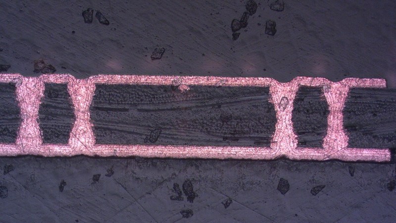
It’s a copper-filled, laser-drilled X-shaped through hole that creates an interconnect between two layers of the PCB. This type of Via can reach an aspect ratio of 2:1, with feature dimensions becoming smaller for both the micro-via diameter and the trace width. Instead of increased reliance on pattern plating processes, the X-shaped Via supports a copper electroplating process that consistently produces void-free copper-filled micro-vias.
Design engineers need to consider all factors affecting the filling process (shape of the through holes, diameter, aspect ratio, pitch, and hole density) in order to utilize the optimum technologies available for ease of fabrication, which in turn can reduce time to market and lower costs.
PCB Technologies’ advanced fabrication capabilities ensure our ability to plate and fill the X-Via using specialized chemical processes. These exclusive processes help generate void-free plating, very low surface copper thickness, and better copper uniformity.
See also: QFN IC Packages
Advantages of copper-filled X-Vias
Copper electroplating is an important micro-via filling process technology used in the fabrication of HDI PCBs and IC packaging substrates.
Advantages include:
- Thermal conductivity: Copper-filled vias increase thermal conductivity, keeping heat away from sensitive areas, resulting in longer life and lower risk of defects. Instead of heat permeating all areas of the PCB, it travels through the copper; away from sensitive components and directed towards special heat dissipating features located elsewhere on the board.
- Excellent signal integrity: Completely filled through-holes offer many advantages, such as better thermal conductivity and improved signal integrity in high frequency boards.
- Reduced EMI: Micro-vias can help to reduce electromagnetic interference (EMI), which occurs when an electromagnetic field affects an electrical circuit; disrupting operation of the electronic device. Micro-vias are especially useful for circuits prone to EMI, as in high-frequency or high-speed applications.
Giving PCB designers every advantage:
Do you need to produce innovative board designs for next-generation thermal technology with improved core-layer structural integrity, or just highly reliable, quality PCBs for prototypes, small, medium, or high volume runs, promising quick turnaround and comfortable pricing?
Take advantage of the advanced capabilities built-in at PCB Technologies — global leaders for All-In-One PCB Solutions, underscored by our unique expertise in handling complex materials, high-density interconnect (HDI) technology, and our in-house cutting-edge equipment that makes almost any project cost-efficient and customer friendly.
High-demand market sectors served by PCB Technologies:
Medical: When it comes to critical functionality and lifesaving technology, PCB Technologies is right there, producing the PCBs that power complex medical equipment such as pacemakers, imaging devices, and patient monitoring systems. The precision and durability of our boards ensure optimum device safety and reliability, which is of paramount importance in healthcare technologies.
Aerospace: The ability to withstand harsh environmental conditions without compromise means PCB Technologies meets the high standards required for space and aviation equipment, including extreme high/low-temperature ranges, radiation, and vibration. The kind of durability our PCBs bring is essential for aerospace applications, where failure is not an option.
Defense: Robust, secure PCB solutions are what PCB Technologies can offer the defense sector. Reliability and performance are critical for both military and communications applications, whereby equipment must operate with flawless precision, even in rugged environments or under unpredictable conditions.
Performance talks:
PCB Technologies has distinguished itself worldwide through our advanced design, manufacturing, miniaturization, and IC packaging capabilities. Our commitment to innovation and quality has ensured we’ve held a position at the forefront of the PCB manufacturing sector — continually evolving to meet the individual needs of our diverse clientele since 1981.
Glad to meet you: Please contact our experts to discuss your project needs with us anytime.