Why Introduce Graphene into Advanced PCBs?
Eran Lipp
|19th November ,2023
What material can be as hard as a diamond? More pliable than rubber; tougher than steel and lighter-weight than aluminum? Graphene —the strongest material on the planet. Its impressive properties make Graphene one of the most promising new nanomaterials for use in advanced PCB technology today.
With almost science-fiction-like characteristics, Graphene is not only the thinnest and one of the strongest materials known to science, it dissipates heat better than any other material and acts as an excellent conductor of electricity.
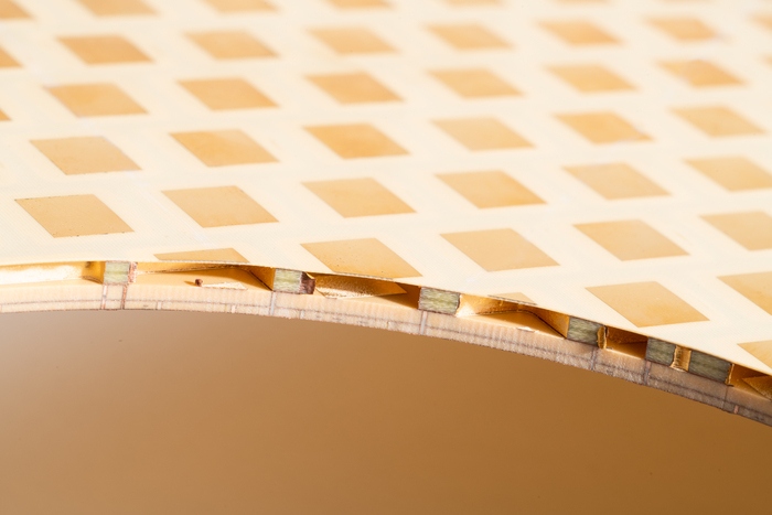
Comprised of a single layer of carbon atoms, bonded in a repeating hexagonal pattern, it takes 3 million one-atom-thick layers of Graphene, stacked one upon the other, to form a 1mm thick sheet of Graphite.
See also:
What makes Graphene attractive to advanced PCB designers?
High electron mobility, one hundred times faster than silicon / The ability to conduct heat as diamonds / Electrical conductivity levels that are far superior to Cu. These attributes translate into some exciting examples of how Graphene can be used to innovative advantage in the production of PCBs:
- Graphene-coated copper traces: Deposited onto copper traces to enhance electrical conductivity and heat dissipation, resulting in faster, more reliable PCBs.
- Graphene-based transistors: Significantly smaller and faster than traditional silicon transistors, opening up new possibilities for super-powerful, ultra-compact electronic equipment
Applications & enhanced functionality
- High-speed digital circuits: Graphene’s high electrical conductivity and low signal attenuation — are ideal for use in 5G communication and data centers.
- RF circuits: Graphene’s low noise and high thermal conductivity — are suited to radar and satellite communication systems.
- Power electronics: Graphene’s high current-carrying capacity and thermal conductivity — benefit power electronics, motor drives and power converters.
- Harsh environments: Graphene’s durability, strength and lightweight — able to withstand the demanding conditions of aerospace and automotive applications.
- Flexible PCBs: Graphene’s inherent lightness and flexibility, — perfect for wearable devices and portable equipment.
- New possibilities: Graphene-based composites, (Graphene combined with polymers or resins) — can be molded or extruded into amazing new board configurations.
-
Challenges working with Graphene
There are however challenges associated with the wider use of Graphene in the PCB industry. On the most basic level, is the fact that large-scale production of Graphene itself involves many complex processes. Because of its low resistance to chemicals, certain processing steps in PCB production may be hampered.
Add to that the higher cost of graphene production, which can include new manufacturing processes, handling and equipment, plus special testing and certification, which may limit applications for PCBs to smaller or medium-volume production runs, at least for now.
A brighter future is being developed
The benefits of Graphene can most definitely outweigh the costs in certain circumstances, such as enhanced performance and efficiency for high-speed and RF applications or the ability to bring to market even lighter and more flexible wearable devices.
Researchers, along with PCB designers and engineers, are currently collaborating to address the difficulties Graphene poses in PCB production through adaptations in current processes and the development of new methods to enable large-scale production of Graphene at lower costs. They are also exploring different types of materials with properties that can protect graphene from chemical reactions.
Blast from our past newsroom: April 2022
PCB Technologies participated in a unique consortium formed between industry-leading companies and academic institutes to introduce Graphene into advanced printed circuit boards.
See a summary below:
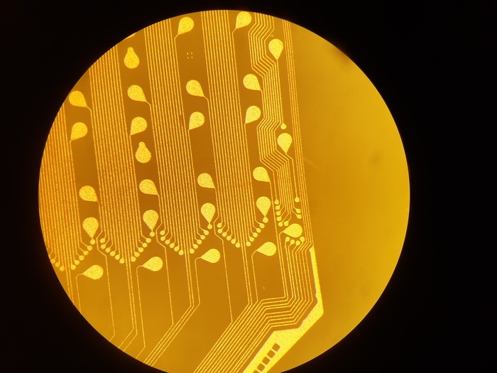
Graphene is a phenomenal 2D material made out of carbon hexagons. Despite its monoatomic thickness, it is extremely strong and has better electrical conductivity than that of metals. This attractive material can be deposited on copper, which is the metal of choice for PCBs, by chemical vapor deposition using methane as a precursor. Graphene/Cu stacks can then be integrated into standard PCB processing to form advanced circuits. Due to its 2D structure and high charge mobility, Graphene improves the circuit performance at high frequency, which is relevant for both RF systems – such as airborne and automotive radars- and for high-speed digital circuits used for 5G communication. Another exceptional property of Graphene is its thermal conductivity, which is 5 times higher than that of copper. This property enables significant improvements in heat dissipation, which is critical for analog high-power devices such as amplifiers and transmitters. Graphene can be included in circuits not only as a layer – Graphene platelets can be mixed into hole-filling epoxy pastes, thus improving the heat conduction of non-plated vias. A fine balance is needed in this case between Graphene and epoxy since a high percentage of the Graphene in the mix results in an electrically conductive paste.
The challenge in working with Graphene is finding a way to include the material on Cu layers without harming its chemical nature by standard processing. As an example, Graphene is not resistant to strong oxidizing agents, such as those critical for surface preparation before drill-hole coating. Exposed Graphene can contaminate electrodeposition baths with carbon or lose its desired properties due to mechanical damage from handling.
So far, we have managed to drill, press, and plate holes in Graphene-including circuits, making the next Graphene patterning phase look promising. This work is done in close collaboration with Prof. Doron Naveh (Bar Ilan University), Prof. Oren Regev, and Prof. Gennady Ziskind (both from Ben-Gurion University).
PCB Technologies All-in-One approach has proved essential in this process, providing decades of experience in using various raw materials and a wide array of engineering capabilities. Read more about our PCB Solutions <<