The Complexities of Microelectronics Microwave Modules
Yaniv Maydar
|1st November ,2023
OVERVIEW
Many factors are driving the rapidly growing demand for high-speed, high-frequency, and wide bandwidth applications in the electronics industry, and it’s creating a sharp increase in the need for high-frequency and millimeter-wave systems, with a view towards providing an ever-widening transmission of data.
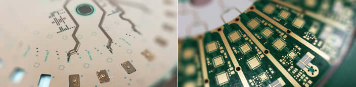
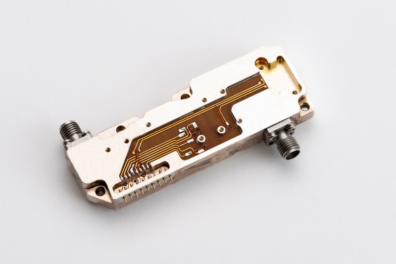
A major consideration is the immediate market need for low-cost, miniaturized systems, which has led to the development of highly integrated, high-frequency technologies such as the Multi-Chip Module (MCM) and System in Package (SiP); systems that operate at frequency ranges between 10 GHz and 100 GHz.
These solutions utilize low-cost ceramic substrates, organic substrates, and PCBs, as well as optimized interconnect solutions and hermetically sealed metal packages, making it possible to implement wider bandwidths with superior electrical performance.
EXPLORING THE COMPLEXITIES
Microwave and millimeter-wave (MVM) frequency package design is a far more complex process than working with lower frequencies. One example of this is in “Distributed Effects.” It becomes an issue at high frequencies because individual feature dimensions can act as active components as the frequency increases or changes.
- INTERCONNECTS: At low frequencies, a wire bond, ball bond, or wedge bond, as well as ribbons and solder ball interconnects, are simply connection points. However, at high frequencies, a wire bond or other interconnect methods perform similarly to that of inductors. At millimeter-wave frequencies, they can even perform as a resonator or an antenna would. Therefore, Distributed Effects issues can dominate design procedures for packaging at high frequencies.
- METAL TRACES: Transmission lines, interconnecting wires, vias, and pins or connectors can act as signal transitions, adding another layer of complexity that affects both the design and manufacturing processes. For example:
- A feature as minute as a bend in a signal trace can degrade performance if not carefully designed.
- A via carrying a signal from one layer to the next can create a signal transition limiting electrical bandwidth.
- MODELING: An extreme effort is often required to accurately model and predict the performance of interconnects and transitions in high-frequency designs. Three-dimensional numerical simulation tools (finite element or finite difference) methods are commonly used.
ADDITIONAL COMPLEXITIES:
Further issues involve the effects of Coupling and Radiation at high frequencies, specifically adjacent metal traces, traces next to integrated circuits, and traces between layers. These traces can couple energy, which can actually be a useful effect. Circuits such as directional couplers and balloons can be created using coupling.
However, coupling is often the hidden enemy of the microwave and millimeter-wave packaging designer. Coupling and radiation effects are difficult to model and need to be dealt with during electrical test procedures. These effects can also lead to resonance, oscillation, and isolation problems.
MATERIALS SELECTION
A critical factor in the high-frequency design process, materials selection, can affect the line impedance and insertion loss of transmission lines. In addition to the material itself, the thickness of both the dielectric and metal layers can influence the design of the transmission lines. Make smart material choices based on the need to minimize interaction with integrated circuits, as in the case of a glob top or under-fill application.
POWER DENSITY
Another major concern often associated with high-frequency components is that of Thermal Power Density. It is particularly problematic for RF power amplifiers that typically have power densities of hundreds of watts per square millimeter. Often in these cases, different design requirements can actually work against one another. For instance, the design requirements for distributed effects and the requirements needed to provide for thermal paths in high-power devices are in direct conflict.
The extreme demands of high-power IC packaging often necessitate designers to become adept acrobats, spending much time and effort balancing numerous conflicting design requirements.
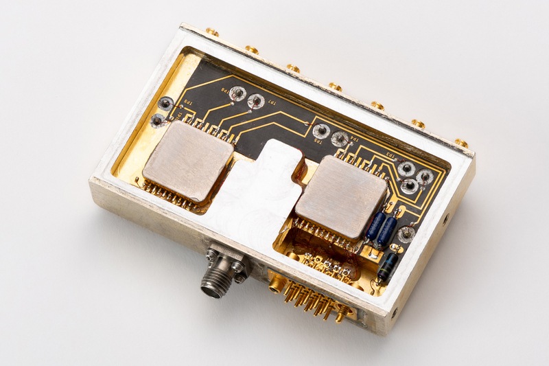
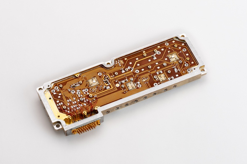
HIGH POWER PACKAGING ISSUES
Concise outline itemizing components for design considerations.
- Materials: Choose for Reliability / Compatibility
- Die Attach:
- Bonding
- Soldering
- Sintering
- Flip Chip
- Interconnect Method:
- Wire Bonding, Ball, Wedge
- Ribbon
- Interposers
- 3D Interconnect, Ball-on- Ball, Standing Wires
- Glass Seal Connectors
- CTE Matching
- Mechanical Design Issues for Hybrid Technology:
- Stages
- PCB
- Ceramic Substrates
- Bare Dies
- SMT
- Sealing:
- Glass Seal
- Hermetic Solder Sealing
- Near Hermetic
- Die Encapsulation:
- Molding
- Glob Top
- Under-fill
When You Think PCB Miniaturization, Think iNPACKTM (A Subsidiary of PCB Technologies). Complete package PCB assembly solutions for both low and high-volume requirements. System-in-Package (SiP) design and manufacturing, surface mount tech, Chip-on-Board (COB), microfabrication, and substrate design and manufacturing capabilities.
We are your dedicated partners across the board, From initial concept to final assembly and beyond. Contact one of our experts to find out how PCB Technologies can help meet your project needs.