PCB Design for Radio Frequency & Microwave Module solutions
Yaniv Maydar
|24th April ,2025
Introduction
Specialized knowledge is required to handle the design, fabrication, and assembly of high-frequency, high-performance PCBs used in sensitive Radio Frequency & Microwave applications. It demands the ability to implement intricate layout techniques, with a deep understanding of complex materials and a mastery over many different thermal management solutions. In addition, careful consideration of design constraints, frequency range, power levels, and other critical factors unique for each application will help safeguard signal integrity and ensure optimal performance.
Learn more about PCB Technology and PCB Manufacturing Processes.
Advantages of Coin Technology for Effective Thermal Management
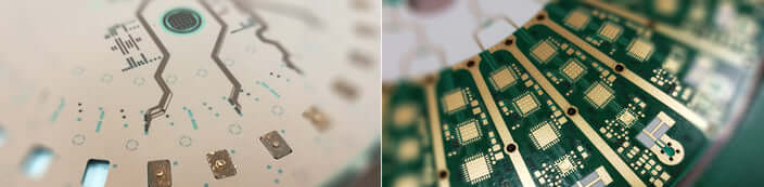
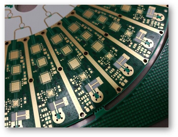
The foremost consideration specific to designing RF/MW boards is the use of controlled impedance lines, the most common being; microstrip, suspended stripline, coplanar waveguide (grounded), and characteristic impedance. Transmission line effects should also be considered; transmission line bends and corner compensation, and layer changes for transmission lines.
Much of PCB Technologies current capabilities are focused on RF & MW PCB design, fabrication and assembly. Controlling line width, thickness, plating and dielectric thickness are critical for board performance, and process variation for these elements will heavily influence electrical performance repeatability. It will also have a direct effect on the power transmitted, losses and therefore, the power dissipated on the board and receiver sensitivity.
As specialists in the field, PCB Technologies offer an impressive range of solutions for Radio Frequency & Microwave Module design by utilizing a variety of materials, hybrid construction boards, tight-tolerance production, the use of air cavities for low Dk transmission lines buried in layers, and controlling bends and corners in line editing.
To top it off, PCB Technologies have developed back-drill capabilities, a unique process for antenna manufacturing that includes phased array antenna design, expertise in the use of low Dk Teflon materials and an integrated solution for power management.
If Radio Frequency & Microwave Module PCB design and functionality is a big part of your world, check out our PCB solutions.