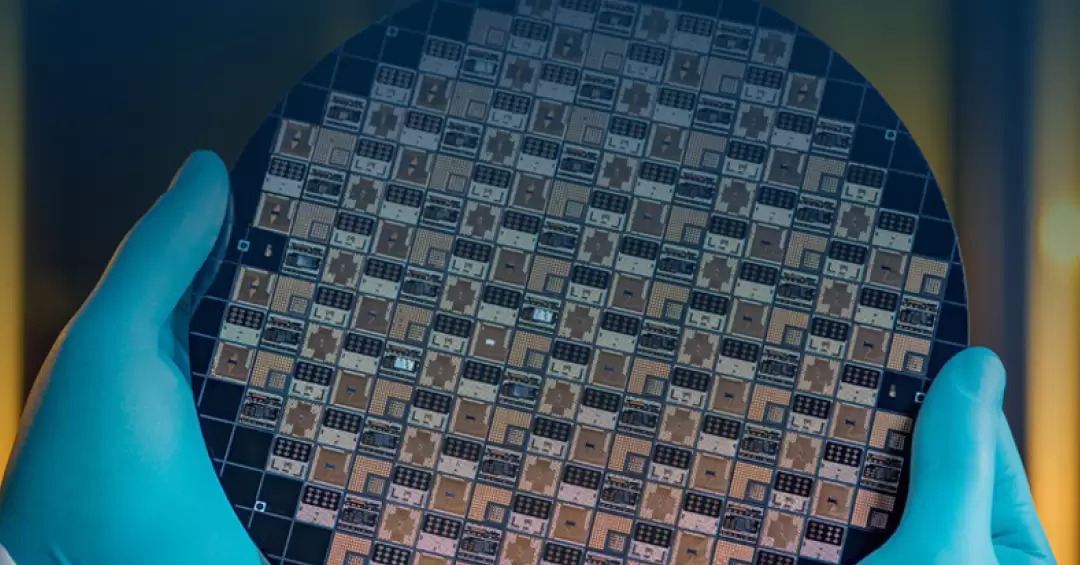
IC Packaging Capabilities
We provide IC packages in a complex array of shapes, sizes, and materials, giving you the ability to select the exact features and functionality best suited to your specific application. This determination however is dependent upon a number of factors, including: Pitch, Dimensions, Lead Count, Thermal Requirements and Costing.
QFN (Quad Flat No Lead), represents a specific IC Packaging solution. iNPACK offers a customized panel-level solution featuring a plastic-encapsulated laminate panel, with a variety of dielectric and CTE options for electrical interconnection with the PCB. This type of packaging can be offered as a full turn-key solution, (including assembly and testing), or as a stand-alone substrate, combined with cavity lid.
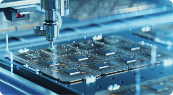
Process & Machinery
SMT P&P
Curing (Flux-less Vacuum Soldering)
Laser Marketing / Labeling / Print
Reflow
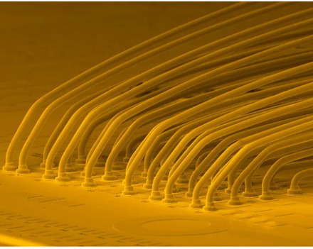
Wedge & Ball
Dicing (Package Sawing)
XRAY
Plasma
Cross Section
Die Attach (soldering and adhesive)
Molding (Encapsulation)
QFN Package
Sintering
Through Mold Interconnection
Dispensing & Stamping
Laser Jet Ball (for BGA)
Laminate QFN Package Types

Dimensions
Pitch
Leads number
Leads number
Lid style
customized
customized
organic/ceramic/glass/metal/molded
General Features
Low profile: 0.9mm for QFN (molded)
Double-staggered lead configuration is an option
Enhanced thermal and electrical performance options available
Cost-effective panel production
ENEPIG and ENIG surface finishes
3x3 to 20x20mm body sizes
0.5 to 260 lead count available
Full in-house design capabilities
JEDEC standard outlines option
Near-hermetic sealing
3D CAD file upon request
Advantages
Material CTE Analysis
to verify that all materials used in the design of interconnections, substrates and thermal interfaces are certified to match the semiconductor properties.
Fanning Out the I/Os
from 2 or more dies to the substrate, which enables chips with improved performance and more I/Os.
Warpage Inspection
for substrate processes in micro assemblies and post SMT processes. Warpage poses a major risk on front and back-end processes, such as ball shooting, mounting, molding and interconnections.
Interconnect Options
are a critical part of packaging. We offer a wide variety of chip interconnect methodologies used in IC package design with an eye towards continuously improved technologies.
Frequently Asked Questions
What processes does iNPACK utilize for die attach?
iNPACK uses eutectic soldering , adhesive, and sintering for die attach.
QFN package, what are the standard pitch and lead count options?
The standard pitch is 0.5/0.65 mm which includes lead count options according to the QFN dimensions.
Beyond standard JEDEC outlines, what level of customization is offered for QFN/LGA packages?
iNPACK offers fully customized dimensions and lead counts for its laminate QFN/LGA packages to meet specific application requirements. iNPACK also provides full in-house design capabilities and can supply a 3D CAD file upon request.
What surface finishes are available for your QFN packages?
The standard available surface finishes are ENEPIG (Electroless Nickel Electroless Palladium Immersion Gold) and ENIG (Electroless Nickel Immersion Gold), as well as unique solutions upon request.
What options are available to enhance the thermal performance of a QFN package?
The options include Controlling dielectrics as well as Cu via fill technology and embedded coin (Cu, CMC).
What technologies are used for creating ball grid arrays and other interconnections?
iNPACK utilizes a Laser Jet Ball process for BGA creation and offers Through Mold Interconnection as another advanced interconnect option.
Can you provide a complete, tested QFN solution, or only the substrate?
iNPACK can deliver a full turn-key solution, which includes the QFN substrate, assembly, and testing. Alternatively, they can provide the stand-alone substrate with a cavity lid.
iNPACK Relevant content
See All Articles
articles
Die Stacking Technology Where Less is Moore in PCB Design & Manufacturing
articles
iNPACK™ Panel Level Solutions
PCB Technologies’ iNPACK Division offers complete package PCB assembly solutions for both low and high-volume requirements. This includes SiP-system in package design and manufacturing, surface mount tech, chip on board (COB), microfabrication, and substrate design and manufacturing capabilities.
articles