Talk to an Expert

LET'S TALK

PCB Solutions

element

We are an All-in-One PCB solutions provider for the fabrication of high reliability, multi-layer, complex boards, PCBA services (supply chain management, assembly, test & inspection, rework & NPI), as well as organic substrates & advanced packaging.

Our global manufacturing capacity meets the highest industry standards backed by a highly experienced team, innovative technologies & advanced processes.

Our heterogeneous engineering turns manufacturers’ reliance on multi-vendor operations redundant while our common design rules allow the development of innovative systems from prototype to low/mid volumes, tailor-made to your needs.

Standards


600 PCB

Rigid PCB

Rigid-Flex PCB

Relevant Applications

  • Industry 4.0

    Fully automated factories relying on data automation efficiency and productivity are constantly increasing their utilization of technological advancements made in autonomous robots, big data, and internet of things (IoT), machine learning, simulation, and system integration. The main incentive of industry 4.0 manufacturers is to track down manufacturing errors as they occur. Big volumes of data analysis require highly reliable PCBs which should be tested and process controlled through each of their production stages. Industries 4.0 also requires PCB design which is able to combine RF, advances processors, antennas, miniaturization, optics and advanced technologies into one integrated system. PCB Technologies is the perfect fit in terms of know-how based on long years of PCB design and manufacturing, PCBA and full system integration.

  • MEMS Devices

    MEMS (Microelectromechanical systems) are the microscopic building blocks of modern electronics. MEMS device, which contains mechanical moving parts within the package, requires proper layout to ensure the highest performance in a finished product. PCB Technologies’ decade-long-experience in PCB design and fabrication contributes to our capacity to provide solutions for the market’s continued demand for miniaturization of electronic devices. We make sure every parameter related to their design does not go unnoticed such as the components sensitivity to mechanical and thermal stress coming from the PCB they’re assembled to, or the need to reduce PCB signal noise to ensure their smooth operation. We implement high-end technologies on accelerometers, gyroscopes, MEMS microphones, motion and pressure sensor modules, and more.

  • Power Devices

    High power devices such as battery chargers, converters, heater controls, inverters, power supplies and switches discharge a large quantity of heat during their operations. Providing the customer with an extreme heat dissipation resistant PCB, while utilizing the PCB as a cooling system requires special expertise. PCB Technologies has the relevant know how in choosing the right materials for the job, as well as the stack up structure, plating, and advanced heating management solutions. We conduct route cause analysis on a regular basis to tackle problems such as repeated delamination between PCB layers caused by the extended heat. It takes a lot of experience in PCB design and fabrication to understand the different environmental conditions in which the PCB operates and its influence on the required heat dissipation solution. We believe getting our engineering team involved in the earliest stages of the PCB design, can serve as a game-changer in both time and money spent.

  • Controller & Motion Systems/C4I Systems

    Under controller systems applications, such as encoder position, piezo motors, servo compensation, step motor stall detection, brushless DC motor commutation, micro-step generation, digital current/torque control, and more, require a unique design and production of PCBs. PCB designs for controllers and motion systems, such as C4I applications, require the ability to support sufficient current to the load, noise immunity for the load, and accurate current sensing. In the case of motion controllers with integrated power electronics, network communications, and derive DC, step motors require specific PCB design rules. Other PCB factors, such as compact size, range of power output levels, vibration, and high level of connectivity make PCB design and manufacturing challenging.

  • Radars

    Radar PCB design requires, among other things, the use of high-frequency PCB materials, such as, teflon, ceramic, and hydrocarbon. This enables the measurement of the distance between objects blocked by electromagnetic wave travel time that the radars are programmed for. Airborne, grid, naval, or land radars, Phased array, as well as Yagi-Uda radar PCBs, all combine various digital and mixed-signal technologies using very high-frequency microwave signals which call for the special know-how and a common design rules kit we possess. PCB Technologies is a world leader in the design and manufacturing of radar PCBs including phased array air cavity antenna designs based on advanced semiconductor technology. This addresses the market’s demand for reduced size, weight, and power consumption of these elements. The next-generation design moves to a flat-panel approach, where each IC is easily mounted on the back of the antenna board allowing large-scale reduction of the antenna’s depth. The integration of higher frequency ICs (GaAs, GaN), makes advanced packaging and thermal management solutions key factor in the production of phased array air cavities to reduce the system’s physical size, improve its long-term reliability, and ensure more than one radiation pattern or data stream as common in conventional dish antennas. We also conduct complex tests and inspection procedures to ensure quality, highly reliable solutions for high reliability and mission-critical applications.

Your Partner for PCB Applications

  • 20 layer stack up, 6 of which are flex layers
  • Raw material - polyamide
  • High-Density PCB – Line/Space 3.5 mil
  • Panel size – 21X30 inch
  • PCB thickness – 3.5 mm
      • Rigid-Flex, Dense BGA, Buried blind, HDI
      • 26 layers, 6 flex layers
      • Sub 2-13, 14-25
      • PCB thickness - 3.34 mm
      • Radio Frequency, Heat sink Solder wave Teflon material (heat sink)
      • Single layer
      • PCB thickness – 0.63mm
      • Rigid-Flex
      • 40 layer
      • Subs – 01-04, 15-26, 37-40
      • PCB thickness – 3.2 mm
      • Rigid-Flex, blind buried, HDI
      • 9 layers, 3 flex layers
      • Sub 2-8
      • PCB thickness 0.6 mm
      • RF, blind, HDI, coin heat sink
      • 12 layers
      • Sub 3-12
      • PCB thickness – 4 mm
      • Rigid-Flex, Buried via
      • 20 layers, 6 flex layers
      • Sub 1-10, 11-20
      • PCB thickness -3.4 mm

    Thermal management

    Thermal management in PCBs ensures that high-power components, such as power amp processors and microcontrollers, maintain safe temperatures by dissipating heat and preventing thermal hotspots. This helps to prevent device failure from overheating. PCB Technologies is an industry leader in thermal management solutions for cooling printed circuit boards (PCBs). As electronic systems and devices become smaller and more sophisticated, so do the components within them which can increase the risk of overheating. In response, we have developed advanced PCB solutions with built-in cooling features that do not add footprint or height to components. With different levels of thermal resistance and cost backgrounds, we have a thermal management solution for every project. These include: • Via farm cooling (filled and capped vias / IPC Type VII / POFV Pre-bonded & soldered) • Heat sinks • Embedded T-coin • Embedded I-coin • Embedded U-coin (Cavity coin) • Post-bonded metal back • Heaters

    High-current PCBs

    Power electronics and high current (up to 1,000 A) use cases require specialist printed circuit boards to manage the voltage distribution. PCB Technologies has many years of experience in the use of embedded copper technology in PCBs for high-current applications. We insert metal, such as copper, into multilayer printed circuit boards. a. Thick Copper We have developed high-tech PCBs that match the current-carrying and heat dissipation qualities of conventional thick copper technology but are lighter, thinner, and more cost-effective. This approach also allows us to combine the embedded copper elements with other technologies like thick copper, embedded coins, HDI, and semi-flex to meet as many needs as possible. Typical use cases for high current PCBs include relay and fuse boxes, DC/DC converters, inverters for renewable energy, and realization of power and signal on one board. b. Embedded coins Utilizing our expert processes, we can insert copper coins or coins made of special materials into any PCB build to meet your specific project needs c. Mixed materials We are experts in the use of mixed and special materials for high-current PCBs including RF laminates, flexible materials, integration of metal parts, HDI and other substrate materials, and low coefficient of thermal expansion (CTE) materials.

    High-frequency PCBs

    High-frequency applications often require the use of special materials for printed circuit boards. 
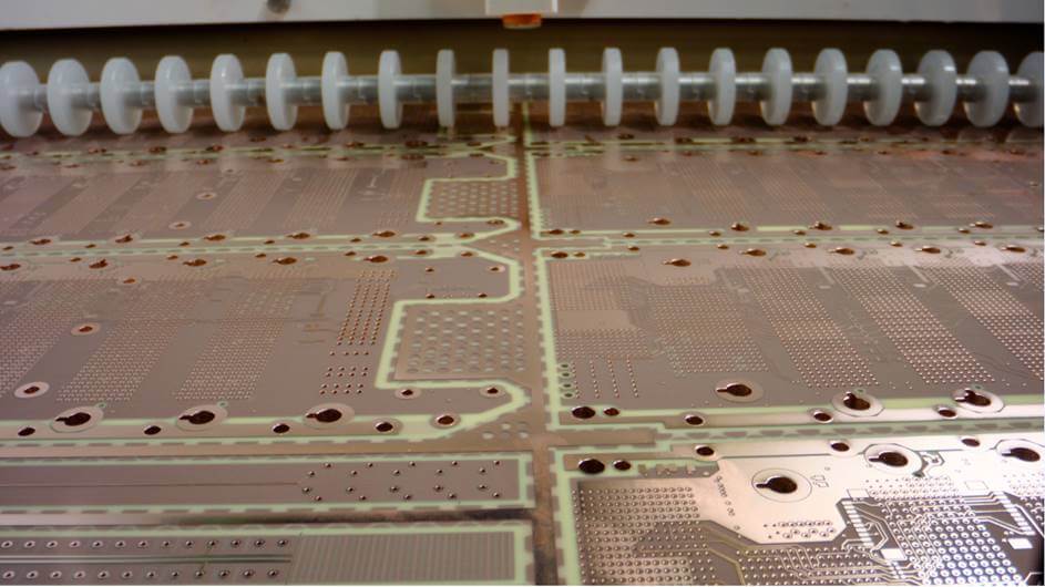
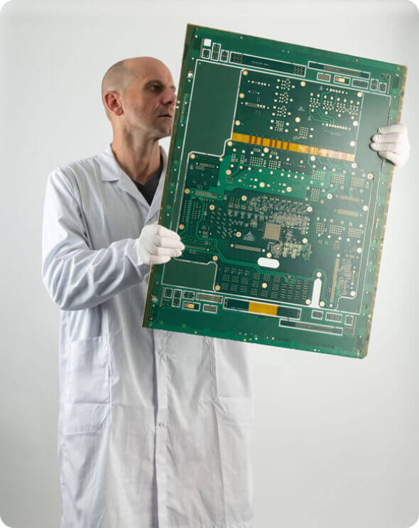
PCB Technologies has a long history in processing PCB base materials, as well as the use of mixed materials, for high-frequency use cases. We use dielectric materials to manufacture multilayer and high-density (HDI) PCBs with high-frequency properties. High-frequency PCB applications include radio, 5G wireless communication, aerospace, sensors for automotive radar, satellites, and other digital applications that require high speeds. a. High density interconnects 
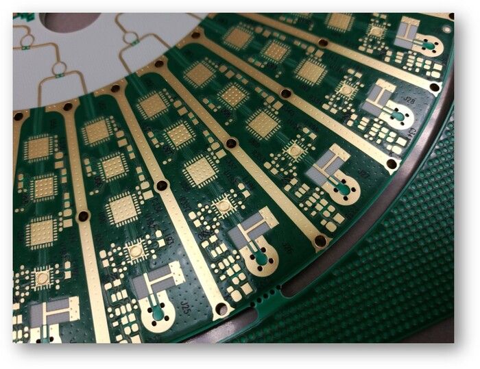
High-Density Interconnect (HDI) printed circuit boards are ideal for high-performance and advanced applications. The higher density structure of these PCB solutions allows for greater complexity and functionality without changing the size of the PCB. This includes the signal integrity and routing required by high-tech devices.PCB Technologies is a market leader in HDI PCB design and manufacture, making use of sequential lamination, high-performance materials, filled microvias, and any layer technology that enables advanced features. HDI PCB applications include 5G wireless communications, IoT devices, medical technology, defense, LiDAR systems, and networking equipment. b. Mixed and special materials 
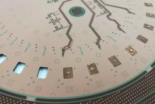
We are experts in the use of mixed and special materials for high-frequency PCBs including RF laminates, flexible materials, integration of metal parts, HDI and other substrate materials, and low coefficient of thermal expansion (CTE) materials. c. Special plating processes As an industry leader in high-tech PCB design, PCB Technologies specializes in special plating processes. Standard: • ENEPIG • ENIG • EPAG (for high speed/RF) • Immersion silver (for RF, high speed, or LF) • Immersion Tin (for LF) • OSP • HAL • Electrolytic Matt Tin (for fluxless soldering) Selective (final finish combinations): • ENIG or ENEPIG with Hard or Soft NiAu • ENIG or ENEPIG with HAL • HAL with Hard or Soft NiAu • ENIG or ENEPIG with Immersion silver • ENIG or ENEPIG with OPS • ENIG with bare copper • Eliminate de-Golding: o Soft Au with 2 different thicknesses [Thin Au - for soldering/wire bond (0.2-0.4 um Au) and Thick Au for very high frequencies (4-6 um Au)] o Electrolytic Matt Tin (for fluxless soldering)

    High-reliability

    As a supplier of printed circuit boards to many demanding industries, PCB Technologies is known for the high reliability of our PCB solutions. Our PCBs go through rigorous reliability testing so that our customers can always depend on their integrity. a. HATS Our in-house fully equipped High Accelerated Thermal Shock Lab allows us to screen out low-reliability materials and processes, as well as detect design issues that may impact reliability. This includes C.A.T. Benchprob & Reflow Simulation testing.

    Advanced IC packaging

    Advanced IC packaging: PCB Technologies offers complete package PCB assembly solutions for both low and high volume requirements. This includes System-in-Package (SiP) design and manufacturing, surface mount tech, chip on board (COB), microfabrication, and substrate design and manufacturing capabilities. Our many years of experience in PCB design and manufacturing means we can create standard and customized substrate solutions for specific use cases and needs. Combining subtractive and MSAP processes with our wide material knowledge, we can solve common challenges such as coefficient of thermal expansion (CTE) mismatches, thermal management problems, and more.

    RF & Microwave

    Radiofrequency (RF) and microwave applications require printed circuit boards that will ensure signal integrity and high reliability. As a global leader in PCB design, PCB Technologies has developed state-of-the-art RF and microwave PCB solutions. Our customers have complete confidence that our PCBs will meet their challenging needs, from aerospace and defense electronics to medical or telecom devices. a. Air cavities b. Cavity & heat dissipation solutions c. Mixed and special materials d. Embedded components

    High-speed PCBs

    Devices that are processing or transmitting high data rates (10Gbit/s or more) require printed circuit boards that can cope with the demands placed upon them. PCB Technologies has experience in developing high-speed PCBs that meet these challenging requirements for functionality and tolerance. This includes signal integrity, impedance match, and insertion loss. Our expertise in material research and development enables us to create PCBs with high layer counts, complex stack structures, low loss, tight dimensions, and more specifically for high-speed use cases. High-speed PCBs are typically used in 5G wireless communication, computing, internet switches, IoT devices, and similar high data rate applications.

    Contact Expert

      0

      This website uses cookies to enhance the user experience.

      Decline

      Thank you

      We will contact you shortly