PCBs – The Critical Core Component in Medical Devices & Equipment

Yaad Eliya
|26th February ,2024
Introduction
The medical device industry is heavily reliant on advancements in PCB technology to generate the kind of life-saving innovations that improve patient care and guarantee better outcomes. Complex PCB component design, coupled with the availability of new composite materials, is driving the evolution of super-miniaturized medical devices and other highly sophisticated medical equipment and machinery.
PCBs used in the design of medical devices must overcome some weighty challenges, such as:
- Miniaturization: Fine line, ultra-flex materials, rigid-flex stack-up, embedded cavities.
- Biocompatibility: Use of materials that are non-toxic or non-adversely reactive to living tissues and biological systems.
- Reliability, repeatability, and uniformity: To ensure consistent functionality time after time.
- CT/MRI: Only paramagnetic metals can be used in the production of PCBs for these machines. Any process, coating, plating, or component with magnetic characteristics (for example, nickel a common plating in PCB production), is definitely not suitable.
This article not only details many of the challenges but also showcases numerous advanced solutions that PCB Technologies brings into play to address them.
Main Challenges for PCBs in the Medical Arena
Challenges can be divided into two categories:
- The use of small or miniaturized PCBs for medical equipment that perform invasive procedures. Materials must be biocompatible with very small fine lines. Types of PCBs most frequently used are flex, multilayer flex, or double-sided flex.
- The use of PCBs in highly sophisticated machines, such as CT and MRI scanners. Not only suitable raw-materials must be utilized in PCB fabrication they must also conform to high reliability (IPC certification) and rapid usability.
Since such medical machines are in service over a span of many years in hospitals and medical centers, their constituent parts must exhibit maximum reliability and repeatability. Year after year, each and every PCB must retain its initial integrity; demonstrating uniform dimensional performance and stability.
PCB Technologies: Advanced PCB Solutions for the Medical Industry
PCB Technologies provides advanced PCB solutions for two main challenges facing the medical equipment industry: PCB Miniaturization required in medical devices and reliability, repeatability, and uniformity in medical instruments/machinery. PCB Technologies is on the certified vendor list of many major medical companies worldwide, such as Philips Medical, Johnson & Johnson, and Biosense Webster.
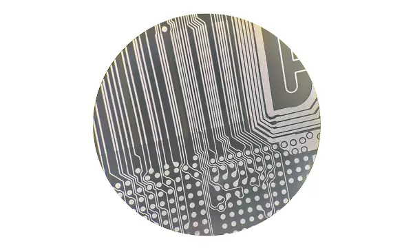
High Resolution Flex Double Side PCB (25/35 um L/S)
PCB Technologies also provides MEMS (Micro Electro Mechanical System) or sensors that are printed on the boards. The challenge here is to produce varied components, like heaters or thermocouples.
The driving force behind the development and use of MEMS is the continued miniaturization in electronics. As the demand for ever smaller electronics grows, PCB Technologies are able to craft smaller components that still retain the ability to operate vital functions. MEMS not only achieve this aim, but also consume less power; allowing for longer operating life.
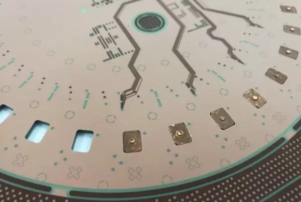
Top View 1 Mil Line Space
The above image is a medical application with a MEMS sensor developed by PCB Technologies along with an R&D company in Israel. The flex board is on a dialysis parasitic piping. The MEMS checks for flow rate temperature and blood pressure traveling through the pipe.
The gray area on the flex double-sideboard is the MEMS itself. The nickel-chrome is actually a buried resistor that helps operate the system. The image illustrates how the board is produced and how it appears with the matrix prior to applying the green solder mask. After applying the flex solder mask on the PCB, we then ship it to the customer to assemble the components.
A second component that we produce is in a copper-nickel alloy called CONSTANTAN, which is like thermal copper. The CONSTANTAN or thermocouple, measures the temperature levels on a PCB. One of the layers in the stack-up is made with CONSTANTAN and not regular copper, able to indicate the temperature on the PCB to prevent system overheating.
Working with Specially Engineered Materials
PCB Technologies has the capability of utilizing specialty materials, not commonly found in PCB production. One such material is ROHACELL®, a (polyetherimide) structural foam extensively used in the aerospace, marine, automotive and medical industries.
In the medical sphere, ROHACELL is used in radomes and mammography plates. Fine-cell materials can be processed by hand lay-up, prepreg, or vacuum infusion techniques at pressures up to 0.3 MPa and temperatures up to 130°C.
How can PCB Technologies serve your needs?
We support our customers across every stage of a project; from the initial PCB design, throughout the fabrication process, and including full-system integration.
Common design rules are maintained, creating the optimal environment for a speedy transformation from prototype to low/mid-range production volumes; eliminating the risk of miscommunication between separate fabrication and PCB assembly shops.
We uphold the strictest standards in quality and production, enabling us provide PCBs of exceptional quality and reliability to serve medical device manufacturers and myriad other industries worldwide.
Contact our technical sales team to discuss how your company can leverage our expertise and agile process design to accelerate your project: Contact PCB Technologies