Subtractive vs. mSAP: Choosing the Right Fabrication Path for Next‑Gen Electronics
Nathan Goldberg
|11th November ,2025
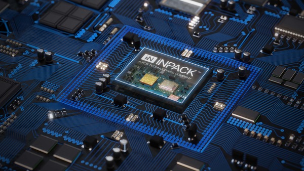
How PCB Technologies + iNPACK Deliver an ‘All‑in‑One’ Approach — from PCB to Package
Executive Summary:
-
- Subtractive etching is mature, scalable and cost‑effective for mainstream HDI.
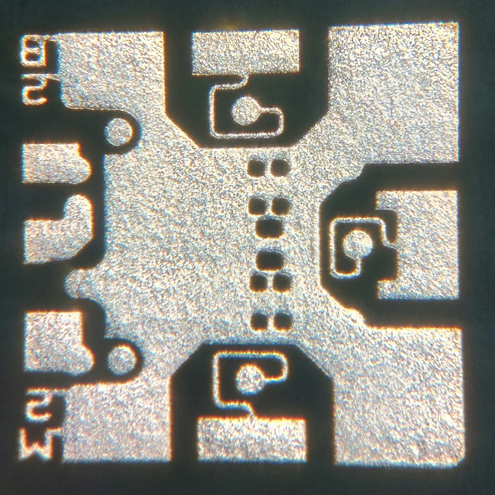
- mSAP (Modified Semi‑Additive Process) unlocks fine‑line routing (≈15–25 µm L/S) with near‑vertical trace sidewalls and tighter impedance control.
- For many programs, the optimal design uses both—subtractive for power/mechanical layers and mSAP for dense SiP, RF or package escape routing.
- PCB Technologies (PCB division) and iNPACK (advanced packaging), provide both capabilities under one roof—reducing hand‑offs, risk and time‑to‑market.
While both Subtractive and mSAP processes use photolithography to define circuit patterns, differences lie in how each process handles material removal and any further fabrication steps required to complete the PCB. mSAP for instance, incorporates additional additive steps to achieve more precise control over circuit features.
Process Steps:
|
Subtractive Process |
mSAP Process |
|
|
mSAP Key Advantages:
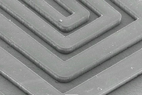
The additive aspects of the mSAP process, allows for more precise control during imaging; achieving finer feature sizes, improved accuracy and reduced material waste. These capabilities are especially advantageous in manufacturing high-density interconnect (HDI) PCBs and substrates.
Process Features:
-
- Fine Pitch & High-Density Traces: mSAP enables the creation of finer and higher-density traces. This is crucial to accommodate PCB designs that require densely packed components and vast numbers of traces.
- Accuracy & Resolution: mSAP enables greater control and precision in defining patterns in copper. This becomes a crucial issue when designing for more complex and miniaturized electronic devices.
- Signal Integrity: The ability to create finer traces and spacing using mSAP technology, allows for improved signal integrity. This is especially important for high-frequency / high-speed electronic applications, where reduced crosstalk and optimal impedance control are critical.
- Thinner Dielectric Layers: mSAP allows the use of thinner dielectric layers between copper layers. These thinner dielectrics contribute to overall miniaturization and are essential in applications with space constraints.
Important Benefits:
-
- Less Material Wastage: Unlike traditional subtractive processes that entail etching away excess copper, mSAP selectively adds copper only to the areas where it’s needed. This results in less material wastage, making the process more environmentally friendly and cost-effective.
- Reliability & Consistency: Enabling more precise control in the fabrication process with mSAP, leads to higher levels of reliability and consistency in the final product. This is critical in applications such as aerospace and medical devices, where reliability is of paramount importance.
- Added Value: Although the initial setup costs for mSAP may be higher than with subtractive processes, for certain applications it can actually be more cost-effective. mSAP technology is proving to be the better option for high-volume production of advanced PCB designs. Adding to that its inherent ability to reduce material waste, can translate into notable cost savings.
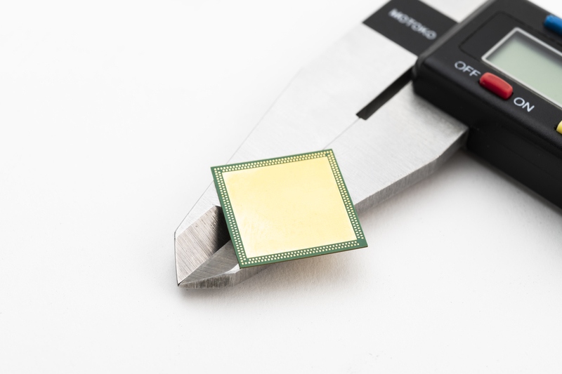
- HDI and Ultra-HDI Compatible: mSAP is well-suited for manufacturing High-Density Interconnect (HDI) boards. mSAP facilitates the kind of intricate circuitry HDI designs require in order to incorporate multiple layers of copper traces and vias within very tight spaces.
Subtractive Etching Key Advantages:
The Subtractive process is a well-established method of producing high-quality PCBs and substrates. While newer processes like mSAP offer certain advantages, subtractive etching is considered the industry standard, applicable for a wide range of PCB designs, from simple single-layer PCBs to more complex multilayer boards.
Production Advantages:
-
- Industry Standard: Most PCB manufacturers are long-experienced in using subtractive processes and have the infrastructure to support it; including etching equipment and waste disposal systems.
- Relatively Simple Setup: subtractive etching typically involves a simpler setup than other more advanced processes, facilitating rapid prototyping and quick production turnaround.
- Material Compatibility: Subtractive technology can handle processing a wide variety of materials, including different types of metals and dielectric materials. This flexibility can accommodate PCB designs with diverse material requirements.
- High Throughput: Subtractive processes can often achieve very high throughput and are well-suited to large-scale production. Familiarity with the Subtractive process and the infrastructure to support it, enables a smoother, more efficient manufacturing workflow.
- Cost-Effective: All of the benefits mentioned above contribute to the popularity of Subtractive processes as a cost-effective method of production for a wide range of PCBs.
Comparison: Subtractive vs. mSAP
While subtractive etching remains a viable production method for many applications, it’s essential to weigh-up factors such as design complexity, precision requirements and budget when making a choice. A more complex fabrication process, like mSAP, is usually preferred in applications demanding high-density circuitry, fine pitch traces or other advanced features; not seen as practical or cost-efficient with subtractive methods alone.
|
Feature |
Subtractive Etching |
mSAP |
|
Process |
Starts with full copper, defines pattern with resist, removes unwanted copper |
Starts with thin seed copper, defines pattern, plates desired traces, removes seep copper layer |
|
Upside |
Mature technology, cost-effective and reliable for simpler designs |
Finer features down to below 25 microns, faster process and less waste |
|
Downside |
Larger features, over 50 microns, complex process, generates more waste | Newer technology, potentially more expensive for simpler designs |
|
Best For |
Simpler designs, lower volume | Complex designs, fine features, high volume (with established mSAP capability) |
PCB Technologies + iNPACK: All-in-One Solutions, from PCB to Package
Most OEMs prefer not to coordinate separate suppliers for medium‑density PCBs, ultra‑fine substrate‑like boards and advanced packages. PCB Technologies and its advanced‑packaging arm iNPACK provide a single, end‑to‑end interface—from subtractive HDI PCBs to mSAP‑enabled fine lines in substrate‑like boards and SiP/IC‑Packaging solutions. This integrated model accelerates development, keeps DFM/DFX feedback loops tight and simplifies qualification across defense, medical and high‑performance electronics.
• PCBs (subtractive & HDI): robust capacity for rigid, rigid‑flex and specialty builds for regulated industries.
• mSAP & substrates via iNPACK: fine‑line build‑up layers, tighter impedance control and package‑level integration for miniaturized RF, sensing and compute modules.
• One team, one QMS: unified engineering, materials and reliability workflows from board to package to system—reducing hand‑offs, risks and time‑to‑market.
Ready to match the right process to your roadmap? Talk to our engineering team about stack‑ups, material sets and test plans that blend subtractive and mSAP imaging where each adds the most value. Contact us at sales@pcb-technologies.com