PCB Manufacturing: Processes, Technologies, Standards
Tal Levy
|5th May ,2025
What is a PCB (Printed Circuit Board)?
A Printed Circuit Board (PCB) is a laminated structure that consists of conductive and insulating layers that serve as the foundation for electronic circuits. The base material (or substrate) is typically fiberglass, which provides both rigidity and thickness. However, flexible PCBs built on high-temperature plastic are also available today.
The History of PCBs
In the past, electronics were designed and assembled from small integrated circuits (ICs) and discrete components. These were connected using wires, and the components were mounted to a rigid substrate. The original substrate was initially a material called Bakelite, which was used to replace the top ply on a sheet of plywood. However, the number of wires required was so great that they often tangled and required vast real estate. This made debugging difficult leading to issues with reliability, the result of which made manufacturing slow.
Early PCBs
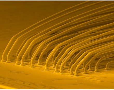
A significant advancement was found in the development of wire wrapping, where a small gauge wire is wrapped around a post at each connection point, creating a highly durable and easily changeable connection. Old PCBs were systems with exposed copper traces and multiple through-holes used to hold large, bulky components. In contrast, modern printed circuit boards have switched largely to surface-mount (SMD) components.
PCB Composition
A PCB includes multiple alternating layers of different materials laminated together with heat and adhesive. Next is the base material, or substrate. The next layer is a thin copper foil, which is laminated to the board with heat and adhesive. The layer on top of the copper foil is called the solder mask layer, which gives the PCB its green (or red) color. It insulates the copper traces from accidental contact with other metal, solder, or conductive bits. The white silkscreen layer is applied on top of the solder mask layer, adding letters, numbers, and symbols to the PCB that allow for easier assembly and better understanding of the board.
Types of Printed Circuit Boards
PCBs can be classified into several categories based on their structure and application. The common types include:
-
- Single-sided PCBs: Components mounted on one surface only. The back surface is typically fully copper (ground) and coated with a solder mask.
- Double-sided PCBs: Components mounted on both surfaces. Each surface is defined as a signal layer in the PCB stack-up, so the surfaces will contain traces that carry signals between components.
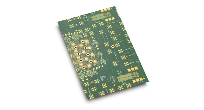
- Multi-layer PCBs (Rigid): Conductors on internal layers that carry electrical signals between components, or the internal layers could be conductive plane layers. Multi-layer PCBs may be single-sided or double-sided.
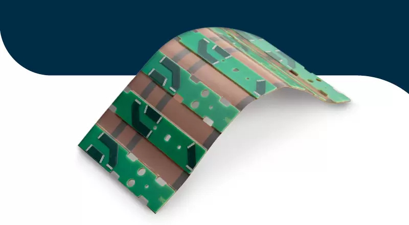
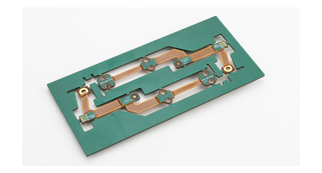
- Flex-rigid PCBs: Use a flexible polyimide ribbon that connects two or more rigid sections in a printed circuit board assembly. These boards might be used when the design must have some movable element, such as a folding or bending enclosure.
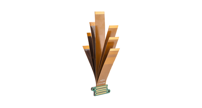
- Flex PCBs: Do not use any rigid materials and are made entirely of flexible polyimide ribbons. These boards can have components mounted and soldered on them, just like rigid printed circuit boards.
Rigid PCB
Flex Rigid PCB
Flex PCB
Electrical Properties
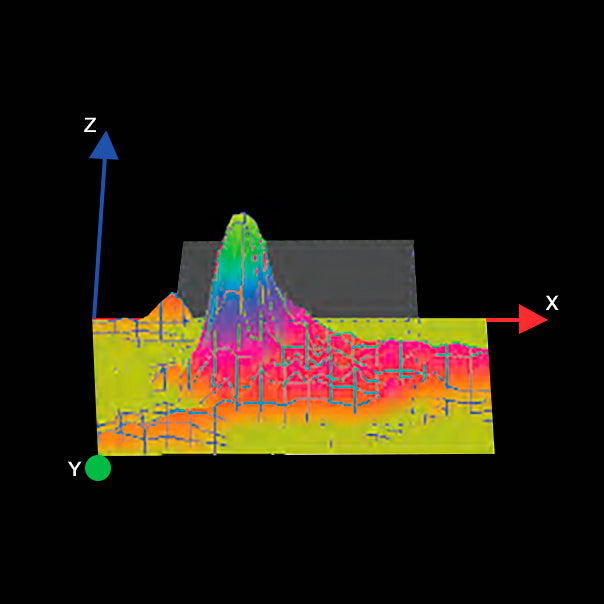
The electrical characteristics of PCBs are determined by their layer stack-up. The structure of layers in a PCB is built with alternating layers of conductive and insulating material, which influences signal and power integrity. For example, a 4-layer structure with internal plane layers (ground and power) helps ensure power integrity while also providing shielding against external electromagnetic interference (EMI).
Laminates and Materials
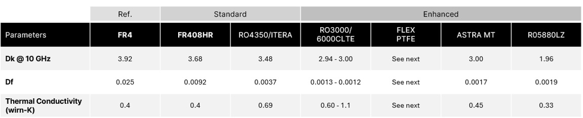
The base material for most PCBs mentioned above is fiberglass, commonly designated as FR4 (Flame Retardant 4), which provides rigidity and thickness. However, several specialized materials can be used based on application requirements:
-
- PTFE laminates: Used in telecom systems requiring low-loss performance in a small package.
- Metal-core PCBs: Use a metal slab in the core layer (normally aluminum) to provide greater rigidity and heat dissipation than typical rigid PCBs. These are common in high-power lighting and some industrial applications.
- Ceramic PCBs: Less common and used in applications requiring very high thermal conductivity to dissipate large amounts of heat from components.
- Flexible polyimide: Used in flex and rigid-flex PCBs, allowing for boards that can bend or conform to specific shapes.
The dielectric and mechanical properties of the core and prepreg (two types of dielectrics used in the layer stack-up) determine reliability and signal/power integrity, making material selection crucial for high-reliability applications such as military and medical devices.
Material -Electrical properties
Printed Circuit Board Terminology
PCBs involve a specialized vocabulary that’s essential for understanding their design, manufacturing, and troubleshooting processes. This glossary covers the most common terms you’ll encounter when working with PCBs, from basic components to manufacturing techniques.
20 Essential PCB Terms
1. PCB (Printed Circuit Board): A board containing conductive material and components that work together to produce a designed electronic function.
2. Copper Weight: Indicator of copper foil thickness on each PCB layer, typically expressed in ounces of copper per square foot.
3. Double-Sided PCB: A board with traces and pads on both sides rather than just one side.
4. FR4: The most used PCB substrate material, a flame-resistant fiberglass reinforced epoxy laminate.
5. Gerber File: A standard file format used to communicate board specifications with manufacturers for controlling photoplotters.
6. HDI (High-Density Interconnector): Advanced PCB fabrication technology using micro blind vias to create boards with high trace density.
7. Multi-Layer PCB: A PCB with at least three conductive layers of traces and components.
8. Pad: A contact point used to connect components with vias and where components are soldered.
9. Plated-Through Hole (PTH): A hole plated with conductive material so that the hole wall becomes conductive, often used as a contact point for through-hole components.
10. Silkscreen: A layer of epoxy ink applied to a PCB containing component names and positions to guide assembly and maintenance.
11. Solder Mask: A layer of epoxy resin applied to the PCB to insulate traces and prevent shorts, typically green but also available in other colors.
12. Substrate: The base material for PCB fabrication, which can be flexible or rigid and is made of materials like epoxy, metal, or ceramic.
13. Trace/Track: Copper paths printed on a PCB that function like electrical wires, connecting components.
14. Via: Plated through-holes that connect signals between traces on different PCB layers.
15. Blind Via: A through-hole that connects inner layers but is not visible from the exterior of the PCB.
16. Impedance ControlL Design technique ensures consistent resistance in high-speed signal traces, important for signal integrity.
17. Dielectric:The insulating layer between copper layers in a PCB that affects capacitance and signal performance.
18. Stencil: A metal sheet used during solder paste application to ensure accurate paste deposition for SMDs.
19. Panelization: The process of grouping multiple PCBs into a single manufacturing panel to improve production efficiency.
20. Thermal Relief: A patterned connection between a pad and a copper pour to control heat flow during soldering. See also: Thermal PCB Management
How to Design a Printed Circuit Board
PCB manufacturing transforms electronic designs into functional hardware through a precise, multi-step process that combines chemical, mechanical, and electronic engineering techniques. Each stage, from initial design to final assembly, builds upon the previous one to create the intricate circuit boards that power all modern electronics.
Here are the steps:
Create the Schematic
A schematic is the electronic blueprint that defines how components will be connected. Using specialized EDA software, designers create a diagram that represents the circuit’s electrical connections using standardized symbols for components like resistors, capacitors, and integrated circuits. The schematic captures all electrical relationships between components but does not represent their physical layout or size.
Simulate the Circuitry
Simulation software analyzes the schematic to predict electrical behavior, signal integrity, power consumption, and thermal performance. This crucial step helps detect design flaws early, saving time and resources by preventing the fabrication of non-functional boards.
CAD Tool Setup
CAD tool configuration includes defining the board’s physical parameters (dimensions, layer count, stack-up), setting design rules (trace widths, clearances, hole sizes), and establishing grid spacing for component placement and routing.
Develop the Library CAD Parts
Before the physical manufacturing begins, designers must create or obtain component library parts for use in their PCB design software. This critical pre-manufacturing step involves:
1. Creating accurate footprints for each component that will be mounted on the board
2. Developing schematic symbols that represent each component’s electrical function
3. Mapping pins between the schematic symbol and physical footprint
4. Establishing 3D models for components to check mechanical clearances
5. Defining electrical parameters for simulation purposes
PCB Layout:
The PCB layout phase bridges design conception and manufacturing preparation:
1. Setting up the board outline and layer stack according to design requirements
2. Placing components strategically to optimize signal flow and minimize interference
3. Routing traces between components following electrical and manufacturing rules
4. Creating copper pours for power and ground planes
5. Adding mounting holes and mechanical features
6. Performing design rule checks (DRC) to validate manufacturability
7. Generating final manufacturing files including Gerbers, drill files, and assembly drawings
How to Use PCB Tools for High-Quality Design
The best results in PCB manufacturing come from a clear understanding of the following:
-
- Design Rule Configuration: Set appropriate clearances, trace widths, and via specifications based on your manufacturer’s capabilities and your circuit’s requirements
- Layer Stack Management: Carefully plan your layer stack for optimal signal integrity, including proper ground and power planes
- Component Organization: Use logical component placement strategies with attention to thermal management, signal flow, and assembly requirements
- Differential Pair Routing: Maintain length matching and controlled impedance for high-speed signal paths
- Power Integrity Analysis: Utilize integrated simulation tools to identify potential voltage drops or current bottlenecks
- Design for Manufacturing (DFM): Run comprehensive checks to ensure your design meets fabrication specifications before submission
The Process of Printed Circuit Board Manufacturing
The manufacturing of printed circuit boards follows a systematic process that transforms design files into functional electronic boards. Here’s a detailed breakdown of each step in the PCB manufacturing process:
Step 1: Design and Output
The process begins with electronic design automation (EDA) software to create schematics and PCB layouts. Once the design is complete, the data is converted into industry-standard formats like Gerber files, which contain information about trace paths, component locations, and board dimensions.
Step 2: From File to Film
The Gerber files are used to create photographic films that serve as templates for each layer of the PCB. These films contain black and clear areas representing where copper should remain or be removed, creating a photographic negative of each circuit layer.
Step 3: Printing the Inner Layers
For multi-layer PCBs, the inner layer cores (copper-clad laminates) are coated with photosensitive material. The film is placed over these layers, and UV light exposes the photoresist. The areas exposed to light harden, while unexposed areas remain soft, creating a pattern that determines where copper will stay.
Step 4: Removing Unwanted Copper
The boards go through a chemical etching process where chemicals dissolve the copper that isn’t protected by the hardened photoresist. After etching, the remaining photoresist is stripped away, leaving only the desired copper traces on the substrate.
Step 5: Layer Alignment and Optical Inspection
Before layering, each inner layer is optically inspected for defects and alignment. Registration holes ensure precise alignment of all layers. Automated optical inspection (AOI) systems verify that the copper patterns match the original design files.
Step 6: Layer-up and Bond
The inner layers are stacked together with sheets of pre-impregnated epoxy-fiberglass material (prepreg) between them. Copper foil is placed on the outer surfaces. The entire stack is then placed in a lamination press where heat and pressure permanently bond all layers together into a solid board.
Step 7: Drill
Computer-controlled drilling machines create the holes for vias and component mounting. The drill files from the design specify the precise location and diameter of each hole. For high-precision requirements, laser drilling may be used for smaller holes.
Step 8: Plating and Copper Deposition
The drilled holes are metalized through an electroplating process that deposits copper on the hole walls. This creates electrical connections between different layers. Additional copper is then plated onto the entire board surface, building up the traces and pads to the required thickness.
Partnering for PCB Manufacturing Excellence
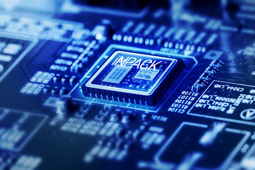
PCB Technologies is an All-in-One Solutions provider of high-mix multilayer rigid, rigid-flex and multi-flex PCBs, Substrates , IC Packaging , complex electronic component assemblies and electro-mechanical sub-systems. We supply it all, from bare board manufacturing to finished electronic products. Customers the world over depend on our full-process, in-house capabilities for everything from quick turn-around of new product prototypes to cost effective mid to high-volume production runs. We’re also specialists in miniaturization and advanced packaging solutions with our exclusive iNPACK technology. The company has become a global front-runner in cutting-edge PCB fabrication; serving myriad industrial sectors including Military/Defense, Aerospace, Medical, RF/Microwave, Robotics/Automation and many others. Precision Circuits Inc. (PCI), a fully owned U.S. subsidiary of PCB Technologies located in Neptune City New Jersey, is responsible for sales, marketing and customer support for the North American market. Holding a manufacturing license agreement (MLA) from the U.S. State Department since 1997, allows PCI to share technical documentation with non-U.S. manufacturers, thus, enabling PCB Technologies to take part in Department of Defense (DOD) programs. Certifications include: NADCAP, AS9100, ISO 9001, ISO 14001, ISO 13485, UL, MIL 50884 (Adhesive & Adhesive less), MIL-PRF 55110 (various materials), Lead-Free – fully compliance with the ROHS regulations
Ready to take your electronic manufacturing to the next level? Contact PCB Technologies today to discuss your specific PCB requirements.