HDI Microvia Technology: The Foundation of Next-Generation Electronic Performance
16th June ,2026
As electronic systems continue shrinking in size while expanding in performance, traditional PCB architectures are approaching their physical and electrical limitations. The demands of AI infrastructure, aerospace systems, defense electronics, medical devices, autonomous systems, high-speed networking, RF communications, and advanced computing are forcing engineers to rethink how interconnect technology is designed and manufactured.
At the center of this transformation is HDI microvia technology.
High Density Interconnect (HDI) PCBs utilizing laser-drilled microvias have become one of the most critical enabling technologies in modern electronics. They allow engineers to achieve greater routing density, improved signal integrity, lower inductance, enhanced thermal performance, reduced layer counts, and dramatically smaller form factors.
But HDI is no longer simply about miniaturization.
Today, HDI microvia technology directly impacts system reliability, high-speed performance, manufacturability, assembly yield, and long-term field performance. Companies developing next-generation products increasingly recognize that successful HDI implementation requires far more than fabrication capability alone. It requires engineering expertise, process control, materials knowledge, and manufacturing discipline.
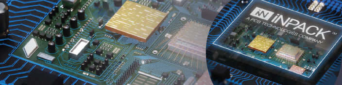
This is where PCB Technologies has established itself as a global technology leader.
What Is HDI Microvia Technology?
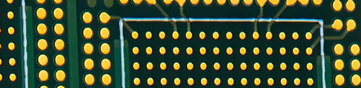
HDI, or High Density Interconnect technology, refers to PCB structures that utilize finer features, smaller vias, tighter spacing, and higher connection pad density than conventional PCB manufacturing.
Microvias are the defining feature of HDI technology.
Unlike mechanically drilled vias, microvias are laser drilled and typically measure less than 150 microns in diameter. In many advanced applications, diameters are significantly smaller. These microvias connect adjacent layers with minimal parasitic effects while enabling substantially higher routing density.
HDI designs commonly include:
- Blind microvias
• Buried microvias
• Stacked microvias
• Staggered microvias
• Via-in-pad structures
• Sequential lamination architectures
• Ultra-fine line circuitry
• High layer count interconnect systems
The result is a PCB architecture capable of supporting extremely dense component packaging while maintaining electrical performance at very high operating speeds.
Modern HDI structures have become essential in applications including:
- AI processors
• Data center hardware
• RF and microwave systems
• Aerospace electronics
• Military systems
• Medical implants
• Wearable devices
• Autonomous vehicle electronics
• High-speed communications
• Advanced sensor systems
Without HDI microvia technology, many of today’s compact high-performance products would simply not be manufacturable.
Why Traditional PCB Structures Are No Longer Enough
Conventional through-hole via structures create numerous limitations as electronic systems become more complex.
Large mechanical vias consume routing space across all PCB layers. This significantly restricts design flexibility and increases layer count requirements. Additionally, traditional vias introduce signal integrity challenges including:
- Increased parasitic inductance
• Higher capacitance
• Reflection issues
• Stub effects
• Crosstalk problems
• EMI concerns
As signal frequencies rise into multi-gigahertz ranges, these limitations become increasingly problematic.
HDI microvias solve many of these issues by dramatically reducing via size, shortening signal paths, minimizing discontinuities, and improving routing efficiency.
For high-speed digital systems, RF applications, and advanced computing platforms, this improvement is no longer optional. It is foundational.
The Engineering Advantages of HDI Microvias
Improved Signal Integrity
One of the most important advantages of microvia technology is enhanced electrical performance.
Because microvias are significantly smaller and shallower than conventional vias, they reduce signal discontinuities and lower parasitic inductance. This becomes critically important in high-speed digital and RF environments where impedance control and signal quality directly affect system functionality.
Microvias also reduce via stub effects, improving eye diagrams, minimizing insertion loss, and supporting higher data transmission rates.
For engineers designing PCIe, DDR memory, RF front ends, aerospace communication systems, or AI processing hardware, HDI structures can dramatically improve overall electrical performance.
Greater Routing Density
As component pitch shrinks, routing channels disappear rapidly.
Microvias restore routing flexibility by allowing traces to escape fine-pitch BGAs and high-density packages more efficiently. This enables engineers to place more circuitry within smaller footprints while maintaining manufacturability.
The ability to fan out dense components effectively is one of the primary reasons HDI technology dominates advanced electronics packaging today.
Reduced Layer Counts
Traditional PCB designs often require additional layers simply to accommodate routing congestion.
HDI architectures frequently reduce overall layer counts through more efficient interconnection strategies. Although HDI fabrication itself is more sophisticated, lower layer counts can partially offset manufacturing costs while improving overall product compactness.
Enhanced Reliability
Properly engineered microvia structures can provide exceptional reliability.
Advanced laser drilling, copper filling, sequential lamination control, and precise plating processes allow HDI boards to withstand demanding thermal cycling and mechanical stress environments.
For aerospace, military, and medical applications, reliability is non-negotiable. HDI manufacturing processes must be tightly controlled to prevent failures such as:
- Microvia cracking
• Corner separation
• Barrel fatigue
• Resin recession
• Copper voiding
• Interconnect separation
This is why manufacturing expertise matters as much as design capability.
Stacked vs. Staggered Microvias
One of the most important design considerations in HDI engineering is the choice between stacked and staggered microvia structures.
Stacked microvias place vias directly on top of one another through multiple layers. This approach maximizes routing density and enables highly compact architectures. However, stacked structures require extremely precise copper filling and plating processes to maintain long-term reliability.
Staggered microvias offset each via between layers. This reduces stress concentration and generally improves reliability while still offering substantial density advantages.
The correct solution depends on:
- Product operating environment
• Thermal cycling exposure
• Layer count
• Signal density
• Reliability requirements
• Mechanical constraints
• Manufacturing capability
Experienced HDI engineering teams evaluate all of these factors before selecting the optimal architecture.
Sequential Lamination and HDI Manufacturing Complexity
HDI PCBs require far more sophisticated manufacturing processes than conventional boards.
Sequential lamination is one of the defining characteristics of advanced HDI fabrication. Multiple lamination cycles allow manufacturers to build complex interconnect structures layer by layer while incorporating buried and blind microvias throughout the stackup.
This process requires extraordinary precision.
Every lamination cycle introduces opportunities for material movement, registration challenges, resin flow variation, and thermal stress accumulation. Maintaining dimensional stability across multiple build cycles demands advanced process control and extensive manufacturing experience.
PCB Technologies utilizes advanced HDI process engineering to ensure precise registration, consistent copper quality, and exceptional interconnect reliability throughout the manufacturing cycle.
Material Selection in HDI Design
Material selection becomes increasingly important as HDI complexity rises.
Engineers must evaluate numerous material properties including:
- Dielectric constant (Dk)
• Dissipation factor (Df)
• Thermal expansion (CTE)
• Glass transition temperature (Tg)
• Moisture absorption
• CAF resistance
• Thermal conductivity
• Mechanical stability
High-speed digital systems often require ultra-low-loss materials to maintain signal performance at very high frequencies.
RF and microwave applications may require highly specialized dielectric materials with tightly controlled electrical properties.
Aerospace and defense applications frequently demand extreme thermal and mechanical reliability.
Selecting the wrong material can compromise performance long before fabrication begins.
Via Filling Technology
Via filling is one of the most critical processes in HDI manufacturing.
Copper-filled microvias improve thermal performance, increase structural integrity, and support reliable via-in-pad designs for advanced BGA packaging.
However, copper filling must be tightly controlled to prevent:
- Voids
• Uneven plating
• Stress concentration
• Delamination risks
• Reliability failures
Advanced plating chemistry, process monitoring, and quality inspection systems are essential for producing robust filled microvias capable of surviving harsh operating environments.
PCB Technologies applies sophisticated plating and inspection methodologies to ensure consistent via integrity across complex HDI structures.
HDI and Thermal Management
As electronic systems become more powerful, thermal management becomes increasingly important.
HDI technology contributes to thermal optimization in several ways:
- Reduced interconnect resistance
• Improved current distribution
• Enhanced copper density
• More efficient component placement
• Better thermal pathway integration
When combined with advanced thermal management techniques, HDI structures help engineers maintain performance stability in compact high-power systems.
This is particularly important in AI processing systems, RF power electronics, aerospace hardware, and military electronics where thermal margins are extremely tight.
Designing for Manufacturability in HDI
One of the most common mistakes in HDI development is designing beyond practical manufacturing capability.
Successful HDI implementation requires close collaboration between design and manufacturing teams early in the development cycle.
Critical DFM considerations include:
- Aspect ratio limitations
• Annular ring requirements
• Copper balancing
• Stackup symmetry
• Drill registration tolerances
• Material compatibility
• Sequential lamination strategy
• Thermal stress management
• Via structure optimization
The earlier manufacturing expertise is integrated into the design process, the greater the likelihood of achieving successful yields, reduced costs, and long-term reliability.
HDI for AI, RF, Aerospace, and Medical Electronics
The future of electronics increasingly depends on HDI technology.
Artificial intelligence infrastructure requires extremely dense interconnect architectures capable of supporting high-speed processors and massive data throughput.
RF and microwave systems demand controlled impedance structures with exceptional signal integrity.
Aerospace and defense electronics require ruggedized HDI architectures capable of surviving severe environmental stress.
Medical electronics demand miniaturization, reliability, and long-term stability in life-critical applications.
Across all of these industries, HDI microvia technology has become a core enabling platform.
Why PCB Technologies Leads in HDI Innovation
Advanced HDI manufacturing requires far more than equipment investment.
It requires engineering depth.
It requires process discipline.
It requires manufacturing experience developed through years of solving complex interconnect challenges.
PCB Technologies combines advanced HDI fabrication expertise with deep engineering support to help customers successfully develop next-generation electronic systems.
Their capabilities include:
- Advanced HDI architectures
• Laser-drilled microvias
• Sequential lamination
• Fine-line circuitry
• RF and microwave technologies
• High-speed digital PCB solutions
• Rigid-flex technologies
• Thermal management expertise
• Advanced assembly integration
• High-reliability manufacturing
Most importantly, PCB Technologies approaches HDI not simply as a fabrication process, but as a complete engineering solution.
Conclusion
HDI microvia technology is no longer an emerging capability. It is now one of the foundational technologies driving the future of electronics.
As systems continue demanding greater speed, higher density, smaller form factors, improved reliability, and enhanced performance, HDI architectures will become even more essential.
But successful HDI implementation requires partnership.
The companies that will lead the future are those that integrate design expertise, manufacturing excellence, materials science, and process control into one unified engineering strategy.
That is exactly where PCB Technologies continues to differentiate itself.
For engineers building the next generation of electronic innovation, HDI microvia technology is not simply a manufacturing advancement.
It is a competitive advantage.