Sensor Technology
From medical diagnostics and industrial automation, to far-flung space exploration, the success of today’s sensor technologies ultimately hinges on the quality of the PCB Design and Fabrication processes invested in producing them.
Sensor Ecosystems – includes flow, image, level sensors, light, motion, positioning and temperature sensors to name a few. Although extremely varied in functionality, they all rely heavily on-data transmissions and analysis gathered from the environment, manufacturing assets and specialized equipment.
Designing PCBs for Sensors – requires meticulous, complex disciplines that factor-in numerous parameters: Environmental influences impacting operation, Form Factor, Power Requirements and Signal & Power Integrity, that can make or break reliability and repeatability for critical (no-fail) applications.
Cost & Efficiency – Expertise in substrate design plus advanced FAB facilities (equipped with best-in-class Film Assisted Molding Machines), produce a wide range of Microelectronics, System-in-Package Solutions and high precision miniaturized sensors, with minimum trace spacing and width. Our common design rules (PCB, Substrate & Packaging) all under one roof, provide high-efficiency services that boost quality, reduce time to market and lower costs.
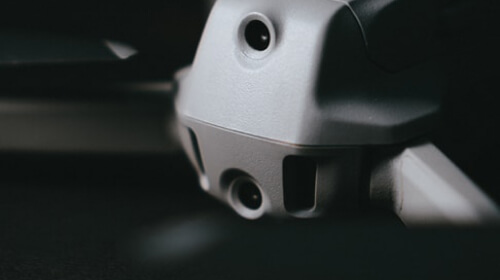
What Does Sensor Packaging Entail?
It’s is a complex form of integrated circuit (IC) packaging that integrates sensors with other components to perform specific functions; requiring electrical connections, structural protection and environmental interfaces.
Key Innovation: MEMS technology enables miniaturized, high-sensitivity sensors, while advanced techniques such as System-in-Package (SiP) and 3D IC stacking allow for the heterogeneous integration of various components into a single, unified package.
Safe-Keeping: Sensor packaging must offer protection from exposure and harsh operating conditions; extreme temperatures, vibrations and corrosive environments. This requires specialized materials and custom design processes to ensure continuous reliability and functionality.
Driving Force: We keep up with rapidly evolving sensor technology by devoting our strategic resources to R&D, as well as investing in advanced manufacturing processes, material sciences, miniaturization, and all-around sensor integration with newer technologies; namely AI, IoT and machine learning.
Types of PCB Sensors
- Temperature Sensors convert temperature changes into electrical resistance/voltage signals (Thermistors, RTDs, Thermocouples). Applications include: HVAC systems, CPUs, battery packs, industrial machinery.
- Pressure Sensors convert pressure into electrical signals to monitor gas or liquid pressure. Applications include: Automotive systems (e.g., tire pressure monitoring), medical devices, industrial automation.
- Motion & Acceleration Sensors measure linear acceleration or angular velocity and function as motion detectors, such as accelerometers and gyroscopes. Applications include: Smartphones, fitness trackers, wearables.
- Gas & Chemical Sensors detect various gases (e.g., carbon dioxide, carbon monoxide, methane, nitrogen dioxide). Applications include: Safety systems, environmental monitoring, smart homes, laboratories or industry.
- Humidity Sensors are embedded in PCBs when accurate environmental readings are necessary. Applications include: Weather stations, agricultural systems, air conditioning systems.
- Light Sensors also referred to as photodetectors, are designed to gauge ambient light intensity. Applications include: Smartphones, streetlights and solar applications for dimming or solar tracking.
- Touch and Proximity Sensors detect physical touch, or the proximity of an object, without actually touching it. Applications include: Robotics, touch screens and smart appliances.
About Us
PCB Technologies is uniquely positioned to offer our advanced design and fabrication capabilities for life-changing Microtechnology applications; specifically, BioMEMS & Sensors; essential in the production of so many new and exciting electronics being introduced into industrial processes and science-based disciplines worldwide.
Along with cutting-edge machinery, PCB Technologies also have the technical power. Our top-tier in-house engineering team is dedicated to supporting customers every step of the way; especially during the crucial early-stage design process.
As an All-in-One PCB Solutions Provider, we cover the entire product development process (all under one roof), making it simpler and easier for our customers to reach their project goals at a reduced time to market and with significant cost savings.
Let’s talk Sensors, Contact Us.