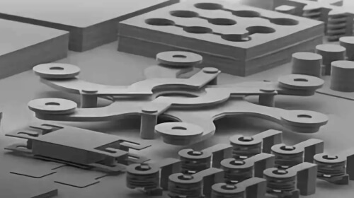
MEMS Devices
Microelectromechanical Systems (MEMS) technology involves creating microscopic devices that integrate combined electrical and mechanical components (sensors, actuators and electronics) on a single silicon chip. These devices integrate a central processing unit (like a microprocessor) with components that interact with the physical world, primarily microsensors and micro-actuators. MEMS are fabricated using modified semiconductor manufacturing techniques, and range in size from one millimeter down to one micron.
Features & Advantages
- Miniaturization: MEMS devices are incredibly small (micrometers to millimeters), allowing for integration into compact electronic systems.
- Batch Fabrication: They leverage the same batch fabrication techniques as integrated circuits (ICs), leading to low per-device production costs and high-volume manufacturing.
- High Performance: Often, micromachined sensors outperform their macroscale counterparts in terms of precision, power efficiency and speed.
- Integration: The ability to integrate mechanical, sensing, and control capabilities onto a single microchip is a core advantage leading to smarter products.
Key MEMS Applications
The MEMS PCB packaging enables peak-performance solutions by delivering ultra-compact, low-power and high-precision systems across many technology sectors.
INERTIAL SENSING & NAVIGATION (IMUS/AHRS): Advanced Gyroscopes, Accelerometers, and Magnetometers combined into Inertial Measurement Units (IMUs), plus Altitude & Heading Reference Systems (AHRS). Navigation Grade MEMS are used in missile guidance, autonomous vehicles, drones and high-precision mapping.
COMMUNICATION & RF: RF MEMS Switches & Filters feature extremely low resistance when ON and very high resistance when OFF, offering high linearity and low power consumption for 5G/6G wireless infrastructure, aerospace and military communications.
OPTICAL SYSTEMS: Micromirror Arrays are essential for LiDAR for autonomous vehicles, High-definition projectors (Digital Light Processing DLP) and optical switches in fiber-optic communication. The James Webb Space Telescope also uses a MEMS Micro-shutter Array to select light sources for spectroscopy.
BIOMEDICAL & HEALTHCARE (BIOMEMS): Lab-on-a-Chip (LOC) Systems use MEMS microfluidic devices (micropumps, microvalves, channels) to handle and analyze minute fluid volumes for diagnostics and drug delivery systems. MEMS are also crucial to Implantable Devices (pacemakers, cardiac monitoring, cochlear implants etc.)
Challenges & Solutions
Because MEMS packaging contains delicate, moving or sensing elements that must interact with external surroundings, they require careful protection from environmental damage. PCB packaging acts as a vital bridge that connects these tiny MEMS die to the larger electronic system, however added safeguards may need to be implemented.
- Stress Isolation: MEMS devices like motion sensors (accelerometers or gyroscopes), are very sensitive to mechanical stress (bending, thermal expansion) from PCB assembly processes (soldering, reflow, housing). The use of low-stress die-attach materials, select PCB materials with a closely matched CTE and symmetrical pad layouts can help mitigate these stresses.
- Environmental Interface & Protection: MEMS devices like pressure sensors, microphones and chemical sensors, interface with their exterior surroundings. The package must provide controlled access: A transparent window for optical MEMS, (MOEMS), or a cavity/port for acoustic or pressure sensors; while also protecting the delicate micro-structures from moisture, contaminants and physical damage.
- Thermal Management: The package must efficiently dissipate heat generated within the device components to prevent performance decay or mechanical distortion in the micro-structures.
- Electrical Connectivity & Noise Reduction: The package must provide robust electrical connections (via wire bonding or flip-chip) and ensure signal integrity. Guidelines recommend using a ground plane directly beneath the MEMS sensor and refraining from routing active signal traces under the package to reduce electrical noise and coupling.
- Miniaturization & Integration: MEMS packaging aims for the smallest possible footprint using techniques like Wafer-Level Packaging (WLP), Chip-Scale Packaging (CSP), or high-density System-in-Package (SiP). SiP involves integrating the MEMS die, an ASIC (Application-Specific Integrated Circuit) and passive components into a single package; reducing overall system size and power consumption.
Meet PCB Technologies’ iNPACK Division
Dedicated to providing our customers with access to high-end technology and innovation such as System-in-Package (SiP) solutions and MEMS Technology.
- Standard & customized substrate solutions: Combining iNPACK’s subtractive and M-SAP processes with PCB Technologies’ extensive materials knowledge, helps us solve common challenges such as coefficient of thermal expansion (CTE) mismatches, thermal management issues, and more.
- iNPACK makes a global impact: Providing SiP, semiconductor packaging, organic substrates (25µm lines and 25µm spacing), and 3-D, 2.5-D and 2-D packaging solutions for aerospace, defense, medical, consumer electronics, automotive, energy and communications industries worldwide.
- Incorporating innovative interconnects: Part of our substrates and micro-assembly process capabilities. These technological solutions can more than double the electronic functionality in the same form factor and create substrate-like PCBs.
- Customer support as it should be: The experts at iNPACK provide support through every stage of the process; design, production and beyond, all under one roof.
Let iNPACK ensure the success of your next project. Contact us to discuss your specifications.