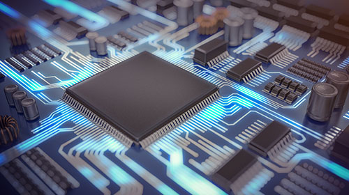
Chip-on-Board (COB)
COB (Chip-on-Board) Technology is an advanced method of packaging electronic chips, especially LEDs, by mounting them directly onto the PCB (sealed with epoxy for protection), instead of in individual packages. COB merges two levels of packaging into one: The chip (component-level) and the PCB wiring (board-level). There’s no need to handle individual packaged components, as everything is combined into a compact, streamlined assembly. This results in faster signal transmission, better thermal control and increased space; allowing designers to pack additional features into ever-slimmer and more powerful devices.
COB Core Advantages
- Direct mounting: Instead of mounting pre-packaged chips, COB technology mounts bare, individual chips directly onto the circuit board. Saves space and reduces weight.
- High chip density: The direct mounting method allows more chip placement in a smaller area, allowing higher resolution and tighter pixel pitch in LED displays.
- Electrical performance: Without individual packaging, COB reduces electrical connection paths, for lower resistance and more effective heat dissipation.
- Cost-efficiency: COB can be more economical than traditional packaging for both small and large production runs.
- Thermal management: Direct bonding allows more heat to be effectively channeled through thermal pads or heat sinks.
PCB Technologies Specializes in COB Technology
Our processes involve mounting bare semiconductors and wires to the PCB surface, while using conductive or non-conductive adhesives, ball bonding, aluminum wedge bonding or die attach, for electrical connections. Our COB technology guarantees a low wire bonding loop profile, higher reliability and advanced capabilities in supporting the intensive use of Input/Output (I/O) modules and systems.
COB assembly for PCBs generally follows two main processes:
- Flip Chip on Board: Where solder is applied directly onto the PCB rather than the chip. The chip is then positioned like a standard surface-mounted device and reflowed along with other components. This process allows for compact configurations, efficient electrical connections and helps improve operational efficiency in high-performance assemblies.
- Wire Bonding: Involves securing the chip to the board with adhesive. Fine wires are welded between each device pad and its corresponding contact on the PCB, then sealed with epoxy. A preferred technique in global manufacturing for high-precision devices.
Accommodating Chip-On-Board Technology
PCB manufacturers must accommodate the needs of COB Technology through specialized design rules, precise manufacturing processes and the use of specific materials to facilitate direct die attachment and wire bonding, followed by encapsulation.
MATERIAL SELECTION
Surface Finish: A specialized surface finish is applied to the pads to ensure reliable bonding. Electroless Nickel Immersion Gold (ENIG) or thicker electroplated gold is typically used, as the gold layer is thicker than standard finishes and provides the necessary energy and robust surface for die bonding.
Substrate Material: While standard FR-4 material can be used for low-cost applications, manufacturers also use more advanced substrates (like polyimide for flexible PCBs or specific materials for high-frequency applications) to meet specific thermal or electrical performance requirements.
Thermal Management Integration: To facilitate the superior heat dissipation qualities of COB, manufacturers can integrate thermal pads or use thermally conductive adhesives or substrates beneath the chip area.
MANUFACTURING PROCESSES REQUIREMENTS
COB Technology requires specialized manufacturing processes because it involves mounting bare LED chips directly onto a circuit board, which demands high precision in processes like die bonding and wire bonding. These processes involve stringent cleanroom environments to prevent contamination and specialized, high-cost equipment for precise placement and encapsulation. The integrated nature of COB makes it difficult to repair, therefore strict manufacturing controls must be in place to prevent defects from the onset.
- Cleanroom Environment: The assembly process often requires a cleanroom environment (typically Class 1000 to Class 10,000) to prevent dust and particulate contamination from interfering with the delicate bare die and wire bonds.
- Precision Die Attach: Specialized, high-precision pick-and-place machines are used to accurately position the bare die onto the PCB using a conductive (silver glue) or non-conductive adhesive.
- Wire Bonding: Manufacturers utilize specific wire bonding machines (thermo-sonic or ultrasonic bonders) to create the electrical connections between the bare chip pads and the PCB traces using ultra-fine gold or aluminum wires.
- Encapsulation (Glob-Top): After bonding, a protective layer of epoxy resin is dispensed over the chip and wire bonds to protect from moisture, dust and mechanical stress. Silkscreen outlines can guide this dispensing process.
- Testing Protocol: Rigorous testing includes thermal and electrical performance checks conducted on the final COB assembly. This Process control step is critical in order to avoid repairs.
Chip-On-Board Applications
Advantages in miniaturization, enhanced thermal performance and durability, have resulted in COB Technology redefining performance and reliability for applications in many industrial sectors.
Lighting Applications:
- Solid-State Lighting (LED): COB LEDs, are a practical solution commonly used in general lighting, street lighting, high bay lighting, track and downlights.
- Large-Scale Displays: Ideal for high-resolution video walls, digital billboards and public information displays. COB LEDs feature tight pixel pitch (high resolution), brightness and durability.
- Photographic lighting: For photographers, stage lighting and film production, COB LEDs offer portability, high-brightness and quality color reproduction.
- Horticulture: COB LEDs enable systems for highly specific, full-spectrum lighting required in producing optimal plant growth and photosynthesis.
Other Essential Applications:
- Medical Devices: COB Technology enables precision, reliability and small form factors in in miniaturized medical devices like endoscopes, monitoring apparatus and diagnostic equipment.
- Communication Modules: In high-speed optical and RF modules for 5/6G base stations, COB Technology meets demands for high frequency, low latency and effective heat dissipation.
- Automotive Electronics: Used in-vehicle displays, headlights/taillights and ADAS sensors, where COB LED’s resistance to vibration and temperature variations are crucial.
- Consumer Electronics: For smaller, lighter devices, COB technology is used in smartphones, tablets and wearables; integrating microprocessors, sensors and memory modules.
What Applications Interest You?
iNPACK (a PCB Technologies Division), is dedicated to meeting your dynamic project needs through advanced capabilities, such as IC packaging and miniaturization micro-processes. We support our customers across the board – from initial design to completed assembly, with technical experts always on-hand to answer your queries.
Moving your projects forward together. Consult with us anytime.