Radar PCB Applications
Radar PCB design focuses on the need for dedicated materials coupled with specialized design expertise due to the very high-frequency microwave signals used in these systems. Basically, Radar systems operate by transmitting and receiving electromagnetic (EM) waves and calculating the travel time for these waves to bounce off objects, which in turn determines the distance to those objects. This functionality places stringent demands on the underlying PCB.
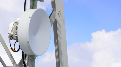
Airborne, grid, naval or land radar, phased-array, as well as Yagi-Uda radar PCBs, all combine various digital and mixed-signal technologies using very high-frequency microwave signals, which require exacting capabilities and a common design rules kit that PCB Technologies is able to provide.
High-Frequency PCB Materials
The most critical requirement for radar PCBs is the use of high-frequency (RF/Microwave) dielectric materials. Standard FR-4 materials are generally unsuitable because they introduce significant signal loss and variations at the microwave frequencies (typically 1 GHz to over 100 GHz) that radar uses.
Key Material Types Include:
- Polytetrafluoroethylene (PTFE) or Teflon: Known for its extremely low dielectric loss tangent (tanδ), which minimizes signal power loss, and a stable dielectric constant (ϵr) across a wide temperature range and frequency spectrum. This makes it a popular choice for high-performance radar.
- Ceramics: Often used in composite materials (ceramic-filled PTFE or hydrocarbon) or as purely ceramic substrates. They offer very stable (ϵr) and excellent thermal conductivity, which is crucial for managing heat from high-power components.
- Hydrocarbon Resins: These are often formulated into specialized laminates that provide a balance of high-frequency performance (low loss) and processing ease, sometimes acting as a lower-cost, high-performance alternative to pure PTFE.
Choosing the right material ensures the integrity of the microwave signal, enabling accurate measurement of EM wave travel time.
Design & Technology Integration
Radar PCBs are complex mixed-signal boards that integrate several distinct technology domains:
- RF/Microwave Front-End: This section handles the high-frequency transmit/receive path and includes components like power amplifiers (PAs), low-noise amplifiers (LNAs), mixers, and filters. This is where the specialized high-frequency materials are most critical, as signal traces must be designed as precise transmission lines (e.g., microstrip, stripline, coplanar waveguide).
- Analog/Mixed-Signal: This involves down-converting the high-frequency RF signal into an intermediate frequency (IF) or baseband signal, and then conditioning it using analog-to-digital converters (ADCs) and digital-to-analog converters (DACs).
- Digital/Processing Backend: This section, typically a high-speed digital board, houses the digital signal processors (DSPs) or Field-Programmable Gate Arrays (FPGAs) that perform the complex algorithms (like Fast Fourier Transform – FFT) to extract distance and velocity information from the digitized radar data.
Specialized Radar PCB Architectures
The principles apply across various radar implementations, requiring tailor-made design rules:
- Phased-Array Radars: These systems use an array of small antenna elements, where the phase of the signal to or from each element is individually controlled. This requires extremely tight phase and length matching on all transmission lines to ensure the antenna array can accurately steer and shape individual or multiple beams electronically.
- Yagi-Uda Radar PCBs: While less common for modern high-resolution systems, a Yagi-Uda antenna (a type of directional antenna) requires specialized transmission line design to connect to the PCB, often at lower frequencies or for simpler applications.
- Application-Specific Radars: The design must adapt to the operational environment, whether Airborne, Grid, Naval, or Land systems. For example, naval and land systems may have more robust environmental sealing requirements, while airborne systems prioritize weight and size constraints.
Key Design Expertise
Successful radar PCB design requires a specific “know-how” and adherence to specialized design rules kit; particularly concerning Signal Integrity (SI) and Power Integrity (PI) at microwave frequencies:
- Impedance Control: Precise control of transmission line impedance (typically 50 Ω) is mandatory. Any deviation can cause reflections, leading to signal loss and inaccurate measurements.
- Crosstalk Mitigation: High-frequency signals can easily couple between adjacent traces. Shielding, proper spacing and ground plane stitching are essential.
- Via Design: Standard through-hole vias can introduce significant inductance and capacitance at microwave frequencies. Low-inductance via designs, such as blind/buried vias and back-drilling, are often necessary to maintain signal quality.
- Layer Stackup: The PCB layer stack-up must be precisely engineered to achieve the required controlled impedance and to provide robust isolation between RF, digital and power layers.
- Thermal Management: Radar systems, especially those using high-power amplifiers (HPAs), generate substantial heat. Effective thermal design, utilizing thermal vias, specialized materials, and heatsink integration, is critical for component reliability and performance stability.
Consult with the Experts
PCB Technologies is a world leader in the design and manufacture of radar PCBs, including phased array air cavity antenna designs based on advanced semiconductor technology. Our next-generation capabilities address market demands for reduced size, weight and power consumption.
Utilization of a flat-panel approach, where each IC is easily mounted on the back of the antenna board, allows large-scale reduction of the antenna depth. The integration of higher frequency ICs (GaAs, GaN), makes advanced packaging and thermal management solutions a key factor in the production of phased array air cavities; reducing the physical size of the system. This improves long-term reliability, especially in multiple data stream radiation patterns. We also conduct complex testing protocols and inspection procedures to ensure full quality compliance.
PCB Technologies provides all-in-one solutions for high-reliability and mission-critical applications. Contact us to find out more.