PCB Heat Dissipation Solutions for High-Performance Systems
Shlomi Danino
|14th May ,2025
As the demand for compact, high-performance electronic systems continues to rise, thermal management has become one of the most technically challenging aspects of printed circuit board (PCB) design. Heat is a natural byproduct of electronic operation, and in the context of high-frequency, high-power, or miniaturized systems, its accumulation can significantly affect system reliability, component lifespan, and overall electrical performance.
Modern applications such as RF modules, power supplies, LED lighting systems, motor controllers, and advanced computing platforms impose thermal loads that must be carefully managed during the design phase. Effective heat dissipation management in PCBs requires a multidisciplinary approach, combining material science, mechanical and electrical engineering, and precision PCB manufacturing technologies.
PCB Heat Dissipation
Thermal Management Techniques in PCBs
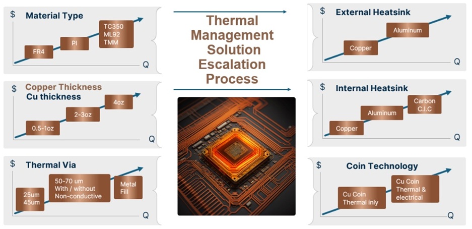
A range of advanced techniques is available for managing heat within PCBs, depending on design constraints, environmental conditions, and the power density of the application. The following are key solutions currently implemented in high-reliability and high-power PCB assemblies:
1) High Thermal Conductivity Prepreg and Dielectric Materials Advanced prepreg materials with enhanced thermal conductivities are used to optimize heat flow within the PCB. For example, materials with Z-axis conductivity of 2.0 W/mK and in-plane (X/Y) conductivity of 3.5 W/mK—approximately 10 times higher than conventional FR-4—can dramatically reduce thermal resistance. Such materials often feature high glass transition temperatures (Tg > 160°C), making them suitable for lead-free assembly and high-temperature environments.
2) Thick Copper Layers Increasing the copper weight on internal and external layers (e.g., 2 oz to 4 oz) allows for higher current carrying capacity and improved heat spreading. This is crucial for power electronics and high-current designs where Joule heating must be minimized.
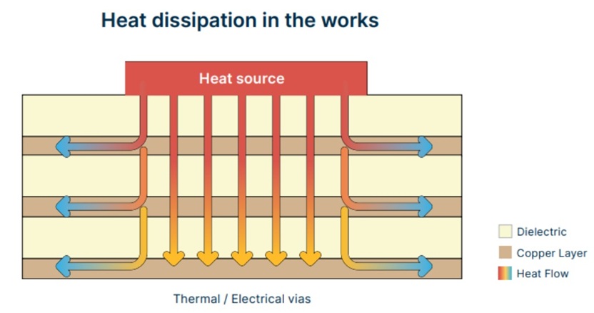
3) Via Farms Thermal vias provide vertical heat transfer paths from surface-mounted components to internal copper planes or external heat sinks. A via farm is a dense array of such vias, electroplated with thick copper between 55-70 µm (typically 35–45 µm), which significantly enhances Z-axis thermal conductivity. This technique is particularly effective when combined with bottom-side heat sinks.
4) Post-Bonded Metal Backing & Thermal conductivity (External solution) A thick metal plate, often copper or aluminum, is bonded to the PCB’s backside after fabrication. This enhances both thermal mass and spreading, and is suitable for boards with asymmetrical heating or where large-area dissipation is needed. Thermal Conductive Adhesives Specialized adhesives such as “Coolspan” are used to thermally couple components or layers while maintaining electrical insulation. Adhesives offer stable performance across a wide range of operating temperatures and are effective in rigid and rigid-flex PCB configurations.
5) Embedded metal layers (Internal solution) Embedded metal layers are internal, usually, copper or aluminum planes integrated within the PCB stack-up to enhance in-plane heat spreading and vertical heat conduction. Unlike external heat sinks or surface-mounted solutions, these internal layers provide a direct thermal path close to heat-generating components. Typically placed beneath power ICs or high-dissipation zones, they function as distributing internal heat sinks and can be electrically isolated or grounded, depending on the design. When engineered correctly, such layers significantly lower thermal resistance across the board without increasing its physical footprint. They are especially effective in multilayer boards where space is constrained, and external dissipation is limited. Material selection and layer positioning are critical—requiring thermal simulation to determine the optimal thickness, metal type, and distance from heat sources.
6) Embedded Metal Coins (T-coin, I-coin, U-coin) Metal coins, typically made of copper or aluminum, are embedded within the PCB stack-up directly beneath heat-generating components. They function as localized thermal spreaders, quickly conducting heat away from critical areas. The shape and size of the coin (T, I, or U profiles) are selected based on thermal simulation and board layout constraints
7) Thermal Design Optimization Beyond physical solutions, effective thermal management also involves layout optimization. This includes the strategic placement of heat sources, use of copper pours for spreading, and simulation of temperature gradients using thermal modeling tools. Controlled impedance routing, particularly in high-speed digital or RF circuits, must be balanced with thermal considerations.
Case Study: High-Thermal-Load PCB Redesign for Military Application
Problem Statement A client required a high-performance PCB capable of operating reliably in an environment with ambient temperatures up to 90°C. The existing 7-layer PCB exhibited repeated delamination due to thermal cycling and insufficient heat dissipation. The original design incorporated a via farm and a bottom-mounted heat sink, but this was inadequate under operational loads.
Initial Analysis Engineering analysis revealed that the prepreg layers used in the original stack-up could not sustain the thermal and mechanical stress. Additionally, pressing the heat sink into the stack-up produced resin flow into the via holes, partially capping them and impairing thermal conduction.
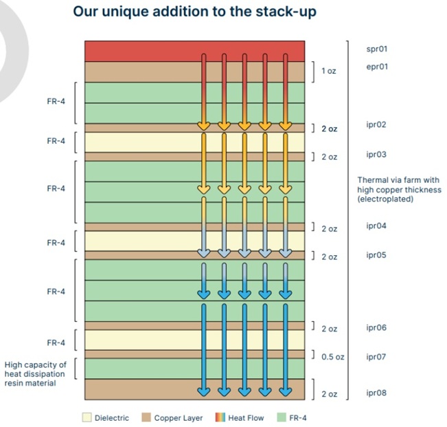
Redesign Approach The redesign introduced an 8-layer stack-up incorporating a custom high-conductivity prepreg material positioned directly under the 7th layer and aligned with the via farm. This prepreg exhibited thermal conductivities of:
-
- Z-Axis: 2.0 W/mK
- X/Y Plane: 3.5 W/mK
- Glass Transition Temperature: 160°C
The copper via farm remained electroplated to 35–45 µm, and the board included additional copper layers (2 oz) to improve lateral thermal conduction. Despite a slight increase in board thickness, the new configuration significantly improved thermal performance.
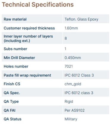
Validation and Performance Results Post-implementation testing included thermal profiling using thermocouples and IR imaging. The new design successfully sustained ambient operating temperatures of 90°C, far exceeding the military specification requirement of 65–71°C. Thermal delamination was eliminated, and component life expectancy improved due to reduced junction temperatures. The board passed IPC 6012 Class 3 and AS9102 quality assurance protocols.
Conclusion
Thermal management in PCBs is no longer optional but a fundamental design requirement, especially for high-power and high-reliability applications. Modern solutions include a combination of structural modifications, high-performance materials, and precise engineering design. These tools allow engineers to effectively dissipate heat, ensuring system stability and durability in demanding environments.
PCB Technologies has developed deep expertise in the field of thermal management through its multidisciplinary engineering teams, access to advanced materials, and a vertically integrated manufacturing process. This allows the company to provide tailored, high-reliability PCB solutions that meet the most stringent thermal and operational requirements.